MIL- STD-883F 2004 TEST METHOD STANDARD MICROCIRCUITS.pdf - 第532页
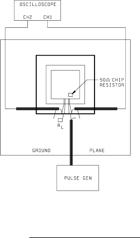
MIL-STD-883F METHOD 3018 29 May 1987 4 FIGURE 3018-1. Test s etup for coupling c apaci tance meas urement .

MIL-STD-883F
METHOD 3018
29 May 1987
3
Connect the pick-up pins to the load resistor and adjust the pulse width so that the time required to charge the coupling
capacitance to 0 V can be observed. Measure the time at the 63 percent voltage point on the waveform (T) and calculate
coupling capacitance (C
c
) as follows:
Determine
R
=
R
x
R
R
+
R
Total
Probe Load
Probe Load
Total
Total
C
=
T
R
C Total Probe
C
=
C
-
C
Values of C
C
can be used as a relative measure for comparison of potential crosstalk among several packages to a standard
package. The coupling capacitance (C
c
) can also be used to predict levels of crosstalk for various logic systems or circuit
configurations by performing a pulse response analysis using a circuit simulator.
3.3 Noise pulse measurements
. Using the same test setup as in 3.2, measure the crosstalk noise pulse voltage at the
minimum noise pulse width specified for the logic system or as specified by the acquiring agency.
Measure the peak noise voltage value of the coupled crosstalk.
4. SUMMARY
. The following details, when applicable, shall be specified in the acquisition document:
a. C
c
.
b. V
OL
(max).
c. V
OH
(min).
d. V
IL
(max).
e. V
IH
(min).
f. t
PL
.
g. t
PH
.
h. t
tLH
.
i. t
tHL
.
j. V
N
.
k. V
NPK
.
MIL-STD-883F
METHOD 3018
29 May 1987
4
FIGURE 3018-1. Test setup for coupling capacitance measurement
.
MIL-STD-883F
METHOD 3019.1
22 March 1989
1
METHOD 3019.1
GROUND AND POWER SUPPLY IMPEDANCE MEASUREMENTS FOR MICROELECTRONICS DEVICE PACKAGE
1. PURPOSE
. This method establishes the means of measuring the series impedance of the ground and power supply
circuit pin configurations for packages used for complex, wide bandwidth microcircuits. The method provides data that are
useful in the evaluation of the relative performance of various packages and can be used to predict the contribution of the
package to power supply noise and ground noise.
1.1 Definition
.
1.1.1 Ground or power supply impedance
. The series combination of inductive reactance and resistance exhibited by all
of the conductor paths between the semiconductor chip interface and the exterior package interface in either the ground
circuit or the power supply circuit. The impedance of a series inductive circuit is defined by the equation:
Z =
R
+
X
L
22
1.2 Symbols
. The following symbols shall apply for purposes of this test method and shall be used in conjunction with the
definition provided in 1.1.
L
G
: Series inductance of the ground circuit path in a package (henries).
L
p
: Series inductance of the power supply circuit path in a package (henries).
X
G
: Series inductive reactance of ground path = 2 π fL
p
(ohms).
X
p
: Series inductive reactance of power supply path = 2 π fL
p
(ohms).
f: Frequency (Hz).
f
tr
: Frequency of primary component of digital pulse transition = 1 (Hz).
t
t
f
tp
: Frequency related to noise pulse width specified for the logic system:
tp
(Hz)
Pmin
f
=
1
t
t
t
: Transition time from logic system. Equal to the smaller value of low to high or high to low transition.
Z
G
: Series impedance of ground path at frequency:
G
2
G
2
G
Z
= R + Z
Z
p
: Series impedance of power supply path at frequency:
p
2
p
2
p
Z
=
R
+
Z
t
Pmin
: The minimum noise pulse width at either the V
IH
or V
IL
level specified for a given logic system.