MIL- STD-883F 2004 TEST METHOD STANDARD MICROCIRCUITS.pdf - 第549页
MIL-STD-883F METHOD 3024 19 August 1994 5 3.2. Ground bounce tes t proc edure . The out put to be t ested s hould be condi tioned t o a low level. The sc ope probe (i f used) s hall be c onnected t o the output under tes…
MIL-STD-883F
METHOD 3024
19 August 1994
4
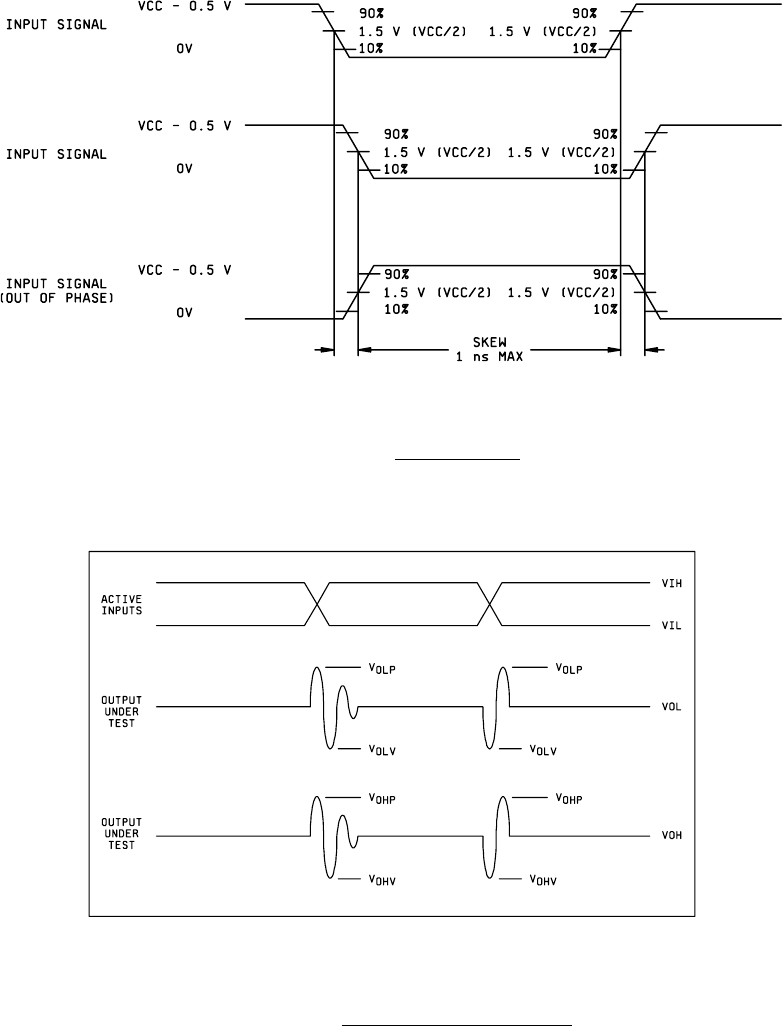
FIGURE 3024-2. Input waveforms
.
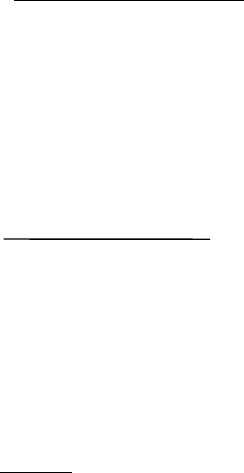
FIGURE 3024-3. Noise measurement technique
.
MIL-STD-883F
METHOD 3024
19 August 1994
5
3.2. Ground bounce test procedure. The output to be tested should be conditioned to a low level. The scope probe (if
used) shall be connected to the output under test no more than 0.25 inches from the pin. The probe ground lead shall be
attached to a suitable location (ground plane or pin) and have a maximum length of 1 inch. The ground bounce noise is the
peak voltage in the positive (V
OLP
) and negative (V
OLV
) directions measured from the nominal V
OL
level (see figure 3024-3).
The noise must be measured at both the LOW to HIGH and the HIGH to LOW transition of the switching outputs. (Two
consecutive areas of disruption need to be analyzed for the largest peak. If a second scope channel is available, it can be
used to monitor the switching outputs and ease synchronization of the noise.) This test shall be repeated with each output
at a low level with all others (functionally possible) switching. The largest peak on the worst output is the device ground
bounce noise. Engineering judgement or experience may be used to reduce the number of pins tested provided that the
rationale for this reduction of pins tested is documented and made available to the preparing activity or the acquiring activity
upon request. (Generally, the noisiest pin on one device will be the noisiest pin on all devices of that type.)
3.3 V
CC
bounce test procedure. The output to be tested should be conditioned to a high level. The scope probe (if used)
shall be connected to the output under test no more than 0.25 inches from the pin. The probe ground lead shall be attached
to a suitable location (ground plane or pin) and have a maximum length of 1 inch. The V
CC
bounce noise is the peak voltage
in the positive (V
OHP
) and negative (V
OHV
) directions measured from the nominal V
OH
level. The noise must be measured at
both the LOW to HIGH and the HIGH to LOW transition of the switching outputs. (Two consecutive areas of disruption need
to be analyzed for the largest peak. If a second scope channel is available, it can be used to monitor the switching outputs
and ease synchronization of the noise.) This test shall be repeated with each output at a high level with all others
(functionally possible) switching. The largest peak on the worst output is the device V
CC
bounce noise. Engineering
judgement or experience may be used to reduce the number of pins tested provided that the rationale for this reduction of
pins tested is documented and made available to the preparing activity or the acquiring activity upon request. (Generally,
the noisiest pin on one device will be the noisiest pin on all devices of that type.)
4. Summary
. The following details, when applicable, shall be specified in the acquisition document:
a. V
CC
Supply voltage.
b. Test temperature.
c. Input switching frequency.
d. Number of outputs switching.
e. Package style of devices.
f. Conditioning levels of non-switching inputs.
g. Output pin(s) to be tested.
MIL-STD-883F
METHOD 3024
19 August 1994
6
This pat intentionally left blank