MIL- STD-883F 2004 TEST METHOD STANDARD MICROCIRCUITS.pdf - 第553页
MIL-STD-883F METHOD 4001.1 22 March 1989 3 3.4 Input offs et volt age drif t . Meas urement of V IO1 is made at temperatur e T 1 in acc ordance wi th 3.1 and a s econd measurement at T 2 of V I02 is made at the sec ond t…

MIL-STD-883F
METHOD 4001.1
22 March 1989
2
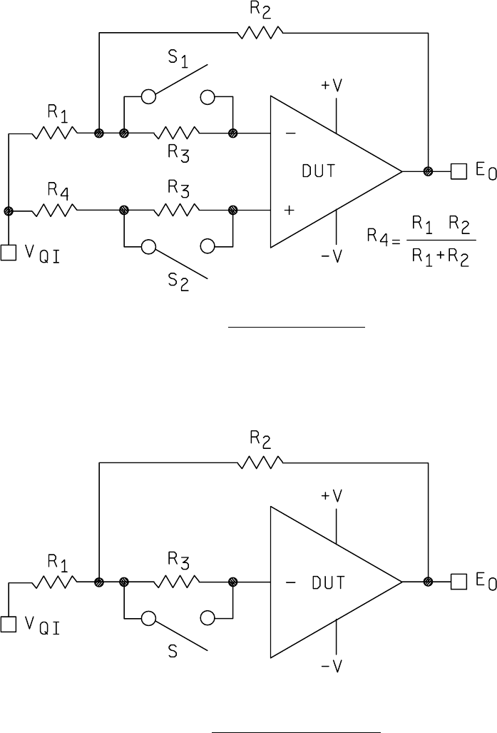
3.2 Input offset current. This has a meaning for differential input amplifiers only.
3.2.1 Differential input amplifier
. The test figure is shown on figure 4001-1. Measure E
01
with S
1
and S
2
closed, measure
E
02
with S
1
and S
2
open.
IO
1
2
01 02
3
I
=
R
R
E
-
E
R
⎛
⎝
⎜
⎞
⎠
⎟
3.2.2 Differential input amplifier using null loop
. The test setup is shown on figure 4001-4, S
1
and S
4
are closed, set
V
C
= 0. Measure E
01
as in 3.1.4. Open S
2
and S
3
and measure E
02
.
IO
1
2
02 01
3
I
=
R
R
E
-
E
R
⎛
⎝
⎜
⎞
⎠
⎟
3.3 Input bias current
.
3.3.1 Differential input amplifier
. The test figure is shown on figure 4001-1. Measure E
01
with S
1
and S
2
closed, measure
E
02
with S
1
closed and S
2
open. Measure E
03
with S
1
open and S
2
closed.
IB+
1
2
01 02
3
I
=
R
R
E
-
E
R
⎛
⎝
⎜
⎞
⎠
⎟
IB-
1
2
01 03
3
I
=
R
R
E
-
E
R
⎛
⎝
⎜
⎞
⎠
⎟
3.3.2 Single ended inverting amplifier
. The test figure is shown on figure 4001-2. Measure E
01
with S closed, measure
E
02
with S open.
IB
1
2
01 02
3
I
=
R
R
E
-
E
R
⎛
⎝
⎜
⎞
⎠
⎟
3.3.3 Single ended noninverting amplifier
. The test figure is shown on figure 4001-3. Measure E
01
with S closed.
Measure E
02
with S open.
IB
1
2
01 02
3
I
=
R
R
E
-
E
R
⎛
⎝
⎜
⎞
⎠
⎟
3.3.4 Differential input amplifier using null loop
. The test setup is shown on figure 4001-4. Set V
C
to zero with S
1
and S
4
closed. Measure E
01
with S
2
closed and S
3
closed. Measure E
02
wth S
2
open and S
3
closed. Measure E
03
with S
2
closed
and S
3
open.
IB+
1
2
03 01
3
I
=
R
R
E
-
E
R
⎛
⎝
⎜
⎞
⎠
⎟
IB-
1
2
02 01
3
I
=
R
R
E
-
E
R
⎛
⎝
⎜
⎞
⎠
⎟

MIL-STD-883F
METHOD 4001.1
22 March 1989
3
3.4 Input offset voltage drift. Measurement of V
IO1
is made at temperature T
1
in accordance with 3.1 and a second
measurement at T
2
of V
I02
is made at the second temperature.
IO
IO2 IO1
21
DV
=
V
-
V
T
-
T
3.5 Input offset current drift
. Measurement of I
I01
is made at temperature T
1
and I
I02
at temperature T
2
in accordance with
3.2.
IO
IO2 IO1
21
DI
=
I
-
I
T
-
T
3.6 Adjustment for input offset voltage
. Use the value of E
0
for 3.1.4. Measure E
01
with the offset null voltage (V
ON
) set to
the positive extreme.
IO Adj O 01
1
2
V
(+) = (
E
-
E
)
R
R
Measure E
02
with the offset null voltage (V
ON
) set to the negative extreme:
IO Adj O 02
1
2
V
(-) = (
E
-
E
)
R
R
NOTE: V
ON
may be implemented using a combination of resistors to obtain the proper voltage across the offset null
terminals. This determination shall be based on the device under test (DUT) specifications.
4. SUMMARY
. The following details shall be specified in the applicable acquisition document for specified values of R
1
,
R
2
, and R
3
, R
4
, R
5
, R
L
, and ±V
CC
of the nulling amplifier.
a. V
IO
maximum.
b. DV
IO
maximum at specified temperature(s).
c. I
IO
maximum when applicable.
d. DI
IO
maximum, when applicable at specified temperature(s).
e. I
IB+
and I
IB-
maximum at specified temperature(s).
f. V
QI
and V
QO
, when applicable, at specified temperature(s).
g. ±V
IO Adj
at specified temparature(s).
h. Test temperature(s). Unless otherwise specified, all parameters shall be measured at the minimum and maximum
specified operating temperature and at +25°C ambient.
MIL-STD-883F
METHOD 4001.1
22 March 1989
4
FIGURE 4001-1. Differential input amplifier
.
FIGURE 4001-2. Single ended inverting amplifier
.