MIL- STD-883F 2004 TEST METHOD STANDARD MICROCIRCUITS.pdf - 第560页
MIL-STD-883F METHOD 4002.1 22 March 1989 4 This page i ntenti onally lef t blank
MIL-STD-883F
METHOD 4002.1
22 March 1989
3
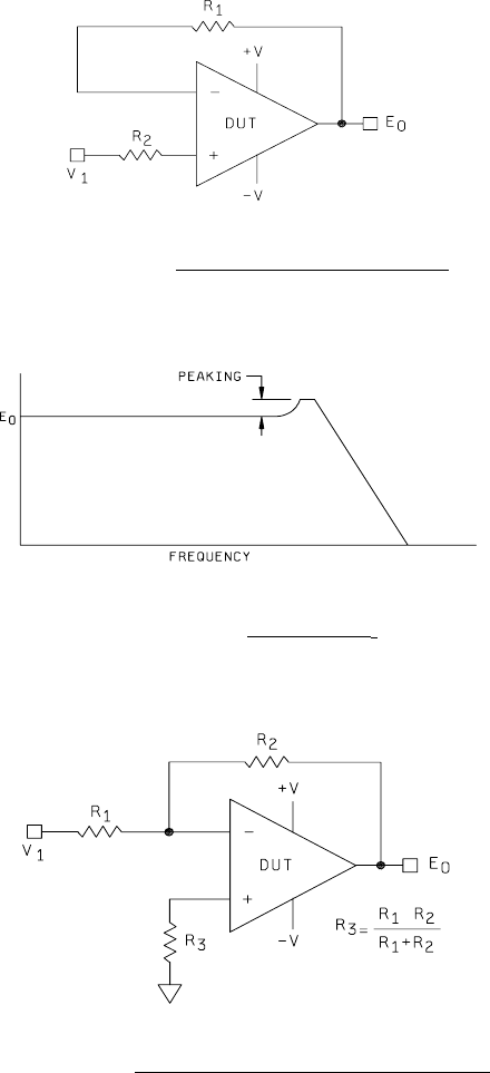
FIGURE 4002-1. Test setup noninverting amplifier
.
FIGURE 4002-2. Amplitude of E
o
.
FIGURE 4002-3. Test setup single ended inverting amplifier
.
MIL-STD-883F
METHOD 4002.1
22 March 1989
4
This page intentionally left blank

MIL-STD-883F
METHOD 4003.1
22 March 1989
1
METHOD 4003.1
COMMON MODE INPUT VOLTAGE RANGE
COMMON MODE REJECTION RATIO
SUPPLY VOLTAGE REJECTION RATIO
1. PURPOSE
. This method establishes the means for measuring common mode input voltage range, common mode
rejection ratio, and supply voltage rejection ratio.
1.1 Definitions
. The following definitions shall apply for the purpose of this test method.
1.1.1 Common mode input voltage range (V
CM
). The common mode input voltage range is that range of common mode
input voltages which, if exceeded, will cause the amplifier to distort or is that range of voltage which may be applied to the
input terminals of the device without decreasing the common mode rejection ratio (CMRR) by more than 6 dB.
1.1.2 Common mode rejecton ratio (CMRR)
. The common mode rejection ratio is the ratio of the differential open loop
gain, A
D
, to the common mode voltage gain, A
C
.
CMRR =
A
A
D
C
CMRR is usually expressed in decibels:
CMRR = 20
A
A
D
C
log
Common mode rejection ratio can also be expressed as the ratio of change in offset voltage to the change in common mode
voltage.
CMRR = 20
V
V
IO
CM
log
∆
∆
1.1.3 Power supply rejection ratio (PSRR)
. The power supply rejection ratio is the ratio of the change in input offset
voltage
∆V
IO
, to the corresponding change in one power supply voltage with all remaining power supply voltage(s) held
constant.
+PSRR =
V
V
V
= constant
IO
CC
BB
∆
∆
- PSRR =
V
V
V
= constant
IO
BB
CC
∆
∆
PSRR =
V
A
V
O
DCC
∆
∆
2. APPARATUS
. The apparatus shall consist of appropriate test equipment capable of measuring specified parameters
and an appropriate test fixture with standard input, output, and feedback resistances.
3. PROCEDURE
. The test figures show the connections for the various test conditions. Assume all switches normally
closed. The feedback resistance, R
2
for figure 4003-1, shall be no larger than the nominal input impedance nor less than a
value which will load the amplifier (100 x Z
OUT
). Specified stabilization and power supply decoupling shall be added where
applicable.