MIL- STD-883F 2004 TEST METHOD STANDARD MICROCIRCUITS.pdf - 第564页
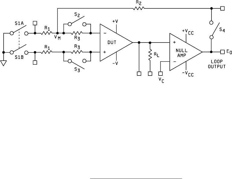
MIL-STD-883F METHOD 4003.1 22 March 1989 4 FIGURE 4003-1. Differ ential input ampli fier us ing null loop .

MIL-STD-883F
METHOD 4003.1
22 March 1989
3
4. SUMMARY. The following details shall be specified in the applicable acquisition document for specified values of C
1
,
C
2
, R
1
, R
2
, R
L,
and ±V
CC
for the nulling amplifier.
a. V
CM
at specified temperature(s).
b. CMRR at specified temperature(s). V
I
signal frequency when applicable.
c. PSRR, when applicable, at specified temperature(s).
d. Test temperature(s). Unless otherwise specified, all parameters shall be measured at the minimum and maximum
specified ambient operating temperature and at 25°C ambient.
MIL-STD-883F
METHOD 4003.1
22 March 1989
4
FIGURE 4003-1. Differential input amplifier using null loop
.

MIL-STD-883F
METHOD 4004.1
22 March 1989
1
METHOD 4004.1
OPEN LOOP PERFORMANCE
1. PURPOSE
. The purpose of this test procedure is to measure gain, bandwidth, distortion, dynamic range, and input
impedance. Gain, dynamic range, and distortion are combined into a large signal test where the distortion measurement will
indicate either lack of dynamic range or inherent distortion.
1.1 Definitions
. The following definitions shall apply for the purpose of this test method.
1.1.1 Maximum output voltage swing (V
OP
). The maximum output voltage swing is the maximum peak-to-peak output
voltage which can be obtained without waveform clipping when the quiescent dc output voltage is set at a specified
reference level. The swing levels are denoted by +V
OP
and -V
OP
.
1.1.2 Single ended input impedance (Z
IN
). The single ended input impedance is the ratio of the change in input voltage to
the change in input current seen between either input and ground with the other input terminal ac grounded. In case of
single input amplifiers, it is the impedance between that terminal and ground. It is measured at the quiescent output dc
level.
1.1.3 Differential input impedance (Z
DI
). The differential input impedance is the ratio of the change in input voltage to the
change in input current seen between the two ungrounded input terminals of the amplifier at the quiescent output dc level.
1.1.4 Voltage gain (A
VS
). The voltage gain (open loop) is the ratio of the output voltage swing to the single ended or
differential input voltage, required to drive the output to either swing limit.
1.1.5 Bandwidth, open loop (BW
01
). The open loop bandwidth is the range of frequencies within which the open-loop
voltage gain of the amplifier is not more than 3 dB below the value of the midband open loop gain.
1.1.6 Distortion
. The total ratio of the RMS sum of all harmonics to the total RMS voltage at the output for a pure sine
wave input.
1.1.7 Unity gain bandwidth (GBW)
: The unity gain bandwidth is the frequency at which the output voltage is equal to the
input voltage.
2. APPARATUS
. The apparatus shall consist of appropriate test equipment capable of measuring specified parameters
and an appropriate test fixture with standard input, output, and feedback resistances.
3. PROCEDURE
. The test figures show the connections for the various test conditions. A differential input is shown, but
if a single ended inverting amplifier is under test, the components shown at the positive input terminal shall not be used. If a
noninverting amplifier is under test, it shall be necessary to either use fixed bias instead of the dc feedback or to use an
inverting gain of one amplifier in the feedback path. For differential output devices, the measurements described in 3.1, 3.2,
3.3, and 3.4 below, as applicable, shall be repeated for the other output using the same test figure except that the measuring
equipment shall be connected to the other output.
3.1 Open loop gain using the null loop
. The test figure is shown on figure 4004-3. The load resistor R
L
is grounded. Set
V
C
to -10 V and measure E
01
. Set V
C
to +10 V and measure E
02
.
VS
2
10201
A
=
R
R
20
E
-
E
3.2 Distortion
. Under the conditions of 3.1, read the distortion on the distortion meter or the voltage at the output of the
rejection filter if that is used.
3.3 Maximum output voltage swing
. The test figure is shown on figure 4004-3. Set V
C
equal to zero. Switches S
1
- S
4
are
closed. For +V
OP
apply a V
1
equal to the positive supply voltage +V
OP
= V
2
. For -V
OP
apply a V
1
equal to the negative supply
voltage -V
OP
= V
2
.