MIL- STD-883F 2004 TEST METHOD STANDARD MICROCIRCUITS.pdf - 第568页
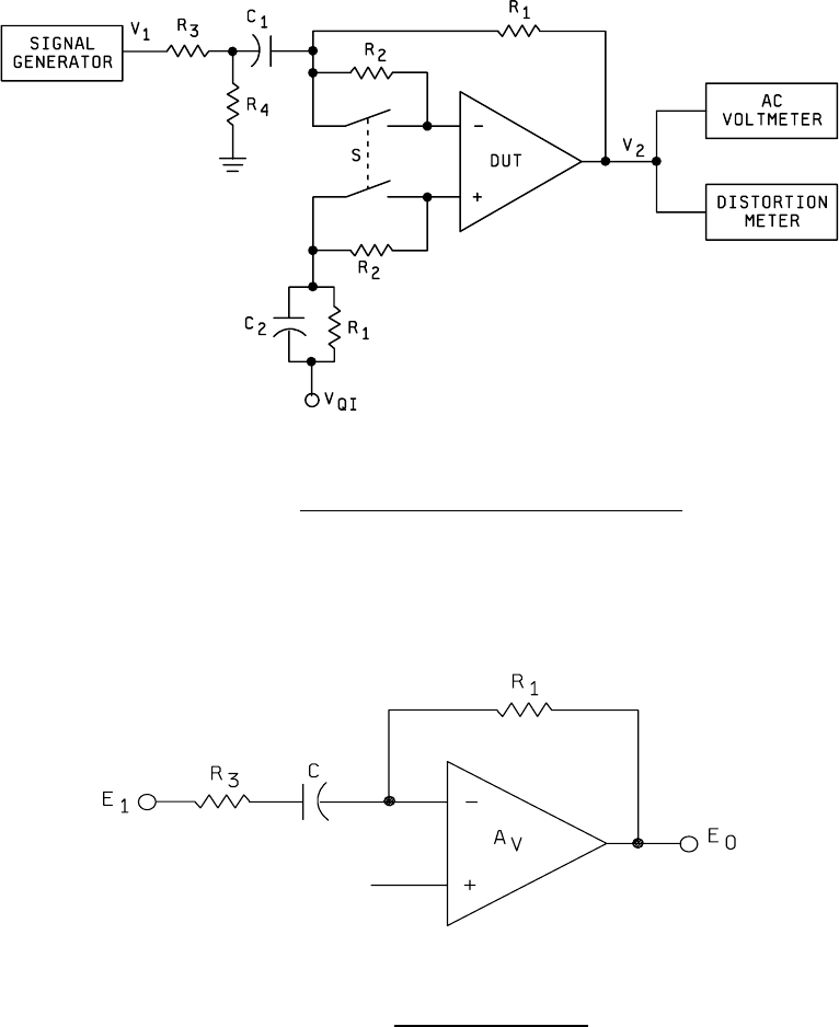
MIL-STD-883F METHOD 4004.1 22 March 1989 4 FIGURE 4004-3. Test s etup for open loop gain, di stor tion and maximum output voltage s wing . FIGURE 4004-4. Test s etup for uni ty gain bandwi dth .
MIL-STD-883F
METHOD 4004.1
22 March 1989
3
FIGURE 4004-1. Test figure for bandwidth and input impedance
.
FIGURE 4004-2. Transfer function circuit
.
MIL-STD-883F
METHOD 4004.1
22 March 1989
4
FIGURE 4004-3. Test setup for open loop gain, distortion and maximum output voltage swing
.
FIGURE 4004-4. Test setup for unity gain bandwidth
.

MIL-STD-883F
METHOD 4005.1
22 March 1989
1
METHOD 4005.1
OUTPUT PERFORMANCE
1. PURPOSE
. This method establishes the means for measuring the power dissipation and output impedance.
1.1 Definitions
. The following definitions shall apply for the purpose of this test method.
1.1.1 Output impedance (Z
0
). The output impedance is the impedance between the output terminal and ground. It is
measured at a specific quiescent dc output voltage and with no ac feedback around the amplifier.
1.1.2 Power dissipation (P
D
). The power dissipation is the total power dissipated in the amplifier with the amplifier biased
into its normal operating range and without any output load.
2. APPARATUS
. The apparatus shall consist of appropriate test equipment capable of measuring specified parameters
and an appropriate test fixture with standard input, output, and feedback resistances.
3. PROCEDURE
. The test figure shown will be used for all three tests. R
1
should be no larger than the nominal input
impedance nor less than a value which will load the amplifier (100 x Z
OUT
). 2 π f R
1
C
1
shall be at least 10 A
D
where A
D
is the
open loop gain and f is the test frequency. C
2
should be at least 10/2 π f R
2
and R
2
should be about equal to the nominal
amplifier Z
0
.
3.1 Power dissipation
. For this test, the signal generator is off. Measure the positive supply voltage and current V
CC
and
I
C
and the negative supply voltage and current V
EE
and I
E
. The power dissipation P
D
= V
CC
I
C
+ V
EE
I
E
.
3.2 Output impedance
. For this test, the signal generator frequency is set to a specified value and the level is set to a
specified V
2
. V
0
is read on the ac voltmeter. The output impedance is then equal to:
O
O2
20
Z
=
V
R
V
-
V
An alternate measurement would be to make R
2
equal to the maximum acceptable value of Z
0
and require that V
0
be no
greater than V
2
/2. For differential output devices, this measurement shall be repeated for the other output using the same
test figure except that the measuring equipment shall be connected to the other output.
4. SUMMARY
. The following details shall be specified in the applicable acquisition document for specified values of R
1
,
R
2
, C
1
, and C
2
.
a. Z
0
limits at the specified frequency.
b. P
D
maximum.
c. V
2
where applicable.
d. V
QI
where applicable at the specified temperature(s).
e. Test temperature(s). Unless otherwise specified, all parameters shall be measured at the minimum and maximum
specified operating temperature and at 25°C ambient.