MIL- STD-883F 2004 TEST METHOD STANDARD MICROCIRCUITS.pdf - 第571页
MIL-STD-883F METHOD 4006.1 22 March 1989 1 METHOD 4006.1 POW ER GAIN AND NOISE FI GURE 1. PURPOSE . The purpos e of thi s tes t proc edure is to measur e smal l si gnal power gai n and the nois e figur e of an amplifie r…
MIL-STD-883F
METHOD 4005.1
22 March 1989
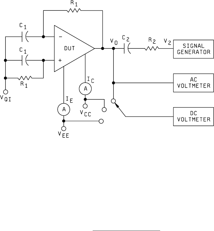
2
FIGURE 4005-1. Test setup-output performance
.

MIL-STD-883F
METHOD 4006.1
22 March 1989
1
METHOD 4006.1
POWER GAIN AND NOISE FIGURE
1. PURPOSE
. The purpose of this test procedure is to measure small signal power gain and the noise figure of an
amplifier.
1.1. Definition
. The following definitions shall apply for the purpose of this test method.
1.1.1 Power gain (PG)
. The power gain is the ratio, expressed in dB, of the signal power developed at the output of the
amplifier to the signal power applied to the input.
PG = 10
P
P
OUT
IN
log
1.1.2 Noise factor (F)
. The noise factor is the ratio of the signal-to-noise power ratio at the input to the signal-to-noise
power ratio at the output.
F =
P
N
P
N
IN
PIN
OUT
POUT
Where: P
IN
= input signal power
P
OUT
= output signal power
N
PIN
= input noise power
N
POUT
= output noise power
1.1.3 Noise figure (NF)
. The noise figure (NF) is the noise factor (F) expressed in dB.
NF = 10 F = 10
P
/
N
P
/
N
IN PIN
OUT POUT
log log
The above expression for NF can be written in terms of voltage since the signal and its associated noise work into the same
load.
NF = 2o
V
N
V
N
= 20
V
N
- 20
V
N
IN
IN
OUT
OUT
IN
IN
OUT
OUT
log log log
Where: V
IN
= signal voltage IN
V
OUT
= signal voltage OUT
N
IN
= noise voltage IN
N
OUT
= noise voltage OUT

MIL-STD-883F
METHOD 4006.1
22 March 1989
2
2. APPARATUS. The apparatus shall consist of appropriate test equipment capable of measuring specified parameters
and an appropriate test fixture with standard input, output, and feedback resistances.
3. PROCEDURE
. The test figures show the connections for the various test conditions. The signal frequency, where
applicable, shall be a specified value within the defined bandwidth of the amplifier.
3.1 Power gain
. Figure 4006-1 is used for this test. Unless otherwise specified, R
2
shall be equal to the nominal output
impedance of the device under test. If the input resistance (R
I
) of the device under test is much greater than the source
resistance (R
G
), unless otherwise specified, a resistor (R) which makes V
I
= 1/2 V
G
should be added in series with R
G
. The
specified ac signal V
G
at the specified frequency is applied to the inputs of the amplifier under test. V
I
and V
L
are recorded.
Then:
PG(db) = 10
V
V
(
V
-
V
)
x
R
R
2
L
IG I
G
2
log
If the series resistor (R) has been added, then:
PG(db) = 10
V
V
(
V
-
V
)
x
R
R
2
L
IG I
1
G
2
log
where:
R
=
R
+ R
1
G
G
3.2 Power gain (insertion method)
. If the input resistance (R
I
) to the device under test is known, the power gain can be
measured by this procedure. On figure 4006-2 with switch S in position 1, and the attenuator set to zero insertion loss, a
reference level is established on the oscilloscope. The switch is then moved to position 2, switching in the circuit under test,
and the attenuation increased until the output is brought to the previous reference level. The voltage insertion gain of the
circuit under test equals attenuator setting in dB. The power gain is then calculated from the following expression:
PG(dB) = (Attenuator reading) + 20
R
(
R
+
R
)
R
(
R
+
R
)
IG 2
2G I
log
where: R
2
equals the nominal output impedance of the circuit under test.
R
G
equals the source resistance.
R
I
equals the input impedance of the circuit under test, unless otherwise specified.
The accuracy of this measurement is dependent upon the accuracy of the attenuator.