MIL- STD-883F 2004 TEST METHOD STANDARD MICROCIRCUITS.pdf - 第573页
MIL-STD-883F METHOD 4006.1 22 March 1989 3 3.3. Noise fi gure . Fi gure 4006-3 i s used f or thi s tes t. The i nput nois e voltage s hall be c alcul ated from t he foll owing expressi on: IN G N = 4 K T f R ∆± where: K …

MIL-STD-883F
METHOD 4006.1
22 March 1989
2
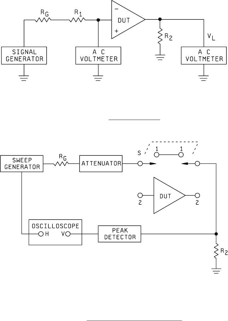
2. APPARATUS. The apparatus shall consist of appropriate test equipment capable of measuring specified parameters
and an appropriate test fixture with standard input, output, and feedback resistances.
3. PROCEDURE
. The test figures show the connections for the various test conditions. The signal frequency, where
applicable, shall be a specified value within the defined bandwidth of the amplifier.
3.1 Power gain
. Figure 4006-1 is used for this test. Unless otherwise specified, R
2
shall be equal to the nominal output
impedance of the device under test. If the input resistance (R
I
) of the device under test is much greater than the source
resistance (R
G
), unless otherwise specified, a resistor (R) which makes V
I
= 1/2 V
G
should be added in series with R
G
. The
specified ac signal V
G
at the specified frequency is applied to the inputs of the amplifier under test. V
I
and V
L
are recorded.
Then:
PG(db) = 10
V
V
(
V
-
V
)
x
R
R
2
L
IG I
G
2
log
If the series resistor (R) has been added, then:
PG(db) = 10
V
V
(
V
-
V
)
x
R
R
2
L
IG I
1
G
2
log
where:
R
=
R
+ R
1
G
G
3.2 Power gain (insertion method)
. If the input resistance (R
I
) to the device under test is known, the power gain can be
measured by this procedure. On figure 4006-2 with switch S in position 1, and the attenuator set to zero insertion loss, a
reference level is established on the oscilloscope. The switch is then moved to position 2, switching in the circuit under test,
and the attenuation increased until the output is brought to the previous reference level. The voltage insertion gain of the
circuit under test equals attenuator setting in dB. The power gain is then calculated from the following expression:
PG(dB) = (Attenuator reading) + 20
R
(
R
+
R
)
R
(
R
+
R
)
IG 2
2G I
log
where: R
2
equals the nominal output impedance of the circuit under test.
R
G
equals the source resistance.
R
I
equals the input impedance of the circuit under test, unless otherwise specified.
The accuracy of this measurement is dependent upon the accuracy of the attenuator.

MIL-STD-883F
METHOD 4006.1
22 March 1989
3
3.3. Noise figure. Figure 4006-3 is used for this test. The input noise voltage shall be calculated from the following
expression:
IN G
N
= 4KT f
R
∆±
where: K = Boltzmann's constant (1.38 x 10
-23
joules/°K)
T = Temperature (
°K)
∆f = Noise bandwidth
R
G
= Source resistance
The input signal level is then set to ten times (20 dB) N
IN
. R
X
is now adjusted so that the ac voltmeter reads 10 dB on some
convenient scale. The input signal V
G
is then reduced to zero and the reduction in dB on the output recorded. The noise
figure NF is obtained by subtracting this drop in dB from 20 dB. The error in this measurement can be calculated from the
following expression:
Error (dB) = 10
V
N
+1 - 20
V
N
2
OUT
OUT
OUT
OUT
log log
⎛
⎝
⎜
⎞
⎠
⎟
⎡
⎣
⎢
⎢
⎤
⎦
⎥
⎥
It should be noted that the error will always be in a direction to indicate a lower noise figure than the true noise figure.
3.4 Noise figure, alternate method
. In this test, a diode noise generator, as shown on figure 4006-4, is used to measure
the noise figure. In this test, with switches S
1
and S
2
in position 1 and the source resistance (R
S
) adjusted to a specified
value, a reference voltage is read on the ac voltmeter. The switches S
1
and S
2
are then moved to position 2 and the diode
source current (I) increased until the previous reference level is read on the ac voltmeter. Using the value of I and R
S
, the
noise figure is determined for the following expression:
NF = 10 Log 20 IR
S
The accuracy of this technique is established by the accuracy of the 3 dB pad and the current meter in the noise diode
circuit.
3.5 Noise factor
. The noise factor can be determined from the following expression:
NF = 10 Log F
In this expression, NF is in dB and F is a numeric.
4. SUMMARY
. The following details shall be specified in the applicable acquisition document for
specified values of R
2
and R
G
:
a. PG, at specified temperature(s) and frequency, and R
2
.
b. NF, at specified temperature(s) and frequency.
c. F, at specified temperature(s) and frequency.
d. Test temperature(s). Unless otherwise specified, all parameters shall be measured at the minimum and maximum
specified ambient operating temperatures and at 25°C ambient.
e. Noise bandwidth (
∆f) (see 3.3).
f. R
S
(see 3.4).
g. R and R
2
, when applicable (see 3.1).
MIL-STD-883F
METHOD 4006.1
22 March 1989
4
FIGURE 4006-1. Power gain test circuit
.
FIGURE 4006-2. Power gain test circuit (insertion method)
.