MIL- STD-883F 2004 TEST METHOD STANDARD MICROCIRCUITS.pdf - 第593页
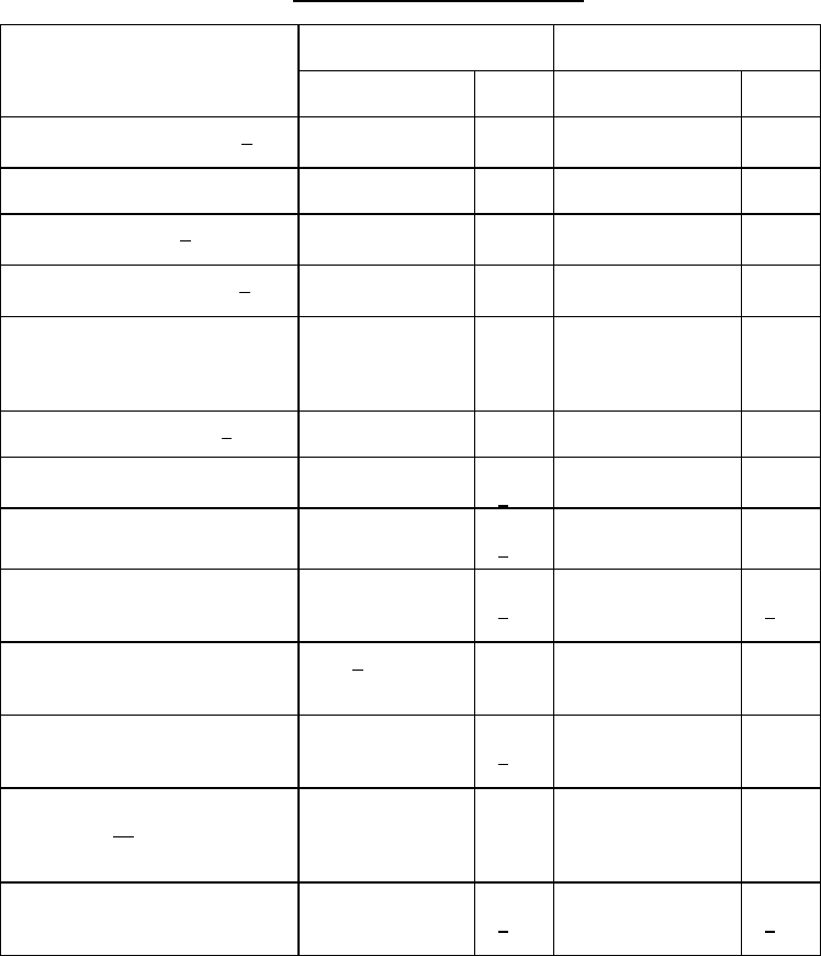
MIL-STD-883F METHOD 5004.11 18 June 2004 3 TABLE I. Clas s l evel S and level B s creeni ng . Screen Class lev el S Class le vel B Method Reqt Method Reqt 3.1.1 W afer l ot acc eptance 1 / 5007 All lots --- 3.1.2 Nondes …

MIL-STD-883F
METHOD 5004.11
18 June 2004
2
3.2 Constant acceleration procedure for large packages (see Table 1, Section 3.1.5). Microcircuits which are contained
in packages which have an inner seal or cavity perimeter of 2 inches or more in total length or have a package mass of 5
grams or more may be treated in accordance with provisions below as an alternate to the procedure of Table 1, Section
3.1.5.
Delete test condition E and replace with test conditions as specified in the applicable device specification. Unless
otherwise specified in the acquisition document, the stress level for large, monolithic microcircuit packages shall not be
reduced below test condition D. If the stress level specified is below condition D, the manufacturer must have data to justify
this reduction and this data must be maintained and available for review by the preparing or acquiring activity. The minimum
stress level allowed is condition A.
3.3 Alternate procedures to method 2010 internal visual for microcircuits
. Alternate procedures may be used on an
optional basis on any microcircuit, provided that the conditions and limits of the alternate procedures are submitted to, and
approved by the preparing activity, or the acquiring activity.
3.3.1 Alternate procedures
.
Alternate 1: The deletions and the changes stated in 3.3.1a are allowable for class level B product only if the
requirements of 3.3.1b and 3.3.1c are imposed and any of the following conditions exists.
1. Minimum horizontal geometry is less than 3 micrometers (µm).
2. Interconnects consisting of two or more levels.
3. Opaque materials mask design features.
a. For inspection of each microcircuit die, delete the inspection criteria of 3.1.1, 3.1.2, 3.1.3, 3.1.4, 3.1.5, 3.1.6, 3.1.7,
and 3.2.5 of condition B of method 2010 and for use in conjunction with alternate procedures add 3.1.1.1, 3.1.1.2,
3.1.1.6, 3.1.3, 3.1.4, and 3.2.5 to the low magnification inspection of method 2010.
b. Temperature cycling (3.1.4). The minimum total number of temperature cycles shall be 50. The manufacturer may
reduce the number of temperature cycles from 50 to the 10 required as part of normal screening based upon data
justifying the reduction in temperature cycles, approved by the preparing activity and an approved plan which shall
include the following criteria:
(1) Reduction of test must be considered separately for each wafer fabrication line and each die family.
(2) The manufacturer shall demonstrate that the wafer fabrication line that produces product which will involve
reduction of temperature cycles is capable and in process control.
(3) The manufacturer shall perform a high magnification visual inspection on a small sample of devices
(e.g., 5(0)) to monitor the process. This inspection may be performed at wafer level.
c. Special electrical screening tests shall be applied to each microcircuit die at the wafer, individual die (chip) or
packaged microcircuit level in accordance with the requirements of 3.3.2 of MIL-STD-883, method 5004. The
conditions and limits of the electrical tests (in table III format) shall be submitted to the preparing activity for
approval and subsequently maintained on file with the qualifying activity. These special screens are in addition to
the required electrical parametric tests which the device must pass and shall be designed to screen out devices
with defects that were not inspected to the full criteria of 3.1.3 (internal visual). Due to the nature of these tests,
they are not to be repeated as part of the qualification and quality conformance procedures in accordance with
method 5005.
Alternate 2: The requirements and conditions for use of this alternate are contained in appendix A of this method.
This option applies to both class level B and class level S microcircuits.
*
*
MIL-STD-883F
METHOD 5004.11
18 June 2004
3
TABLE I. Class level S and level B screening
.
Screen
Class level S Class level B
Method Reqt Method Reqt
3.1.1 Wafer lot acceptance 1/ 5007 All
lots
---
3.1.2 Nondestructive bond pull 2023 100%
---
3.1.3 Internal visual 2/ 2010, test
condition A
100% 2010, test
condition B
100%
3.1.4 Temperature cycling 3/ 1010, test
condition C
100% 1010, test
condition C
100%
3.1.5 Constant acceleration
(see 3.2 and 3.4.2)
2001, test
condition E
(min) Y1
orientation only
100% 2001, test
condition E
(min) Y1
orientation only
100%
3.1.6 Visual inspection 4/
100%
100%
3.1.7 Particle impact noise
detection (PIND)
2020, test
condition A
100%
5
/
---
3.1.8 Serialization
100%
6
/
---
3.1.9 Pre burn-in electrical
parameters (see 3.5.1)
In accordance with
applicable device
specification
100%
7
/
In accordance with
applicable device
specification
100%
8
/
3.1.10 Burn-in test (see 3.4.2) 1015 9/
240 hours at
125°C minimum
100% 1015
160 hours at 125°C
minimum
100%
3.1.11 Interim (post burn-in)
electrical parameters (see 3.5.1)
In accordance with
applicable device
specification
100%
7
/
---
3.1.12 Reverse bias burn-in
(see 3.4.2) 10
/
1015; test
condition A or C,
72 hours at 150°C
minimum
100%
---
3.1.13 Interim (post burn-in)
electrical parameters (see 3.5.1)
In accordance with
applicable device
specification
100%
7
/
In accordance with
applicable device
specification
100%
8
/
See footnotes at end of table.
MIL-STD-883F
METHOD 5004.11
18 June 2004
4
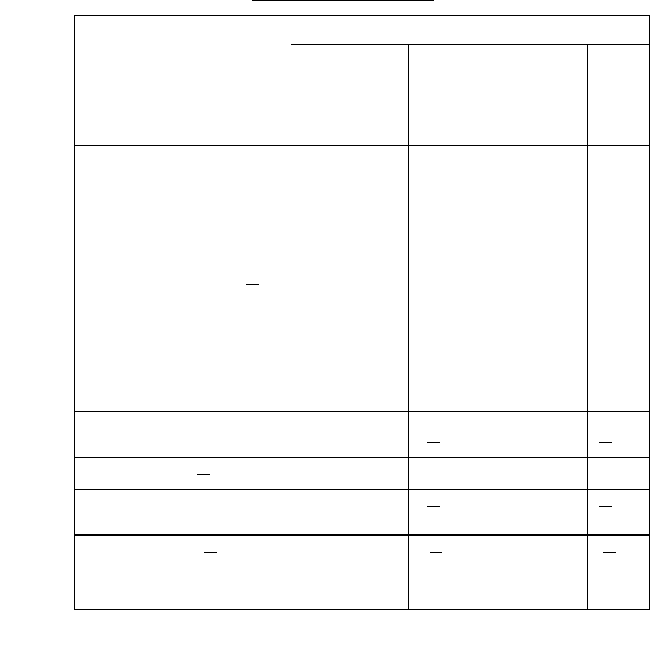
TABLE I. Class level S and level B screening
- Continued.
Screen
Class level S Class level B
Method Reqt Method Reqt
3.1.14 Percent defective
allowable (PDA) calculation
5 percent, see
3.5.1, 3 percent,
functional
parameters at
25°C
All
lots
5 percent, see 3.5.1 All
lots
3.1.15 Final electrical test
(see 3.5.2)
a. Static tests
(1) 25°C (subgroup 1, table I,
5005)
(2) Maximum and minimum rated
operating temperature
(subgroups 2, 3, table I,
5005)
b. Dynamic or functional tests 11
/
(1) 25°C (subgroup 4 or 7,
table I method 5005)
(2) Minimum and maximum rated
operating temperature
(subgroups 5 and 6, or 8
table I method 5005)
c. Switching tests at 25°C
(subgroup 9, table I,
method 5005)
In accordance with
applicable device
specification
100%
100`%
100%
100%
100%
In accordance with
applicable device
specification
100%
100%
100%
100%
100%
3.1.16 Seal
a. Fine
b. Gross
1014 100%
12
/
1014 100%
12
/
3.1.17 Radiographic 13/ 2012 two
views 14
/
100%
---
3.1.18 Qualification or quality
conformance inspection test sample
selection
15/
15/
3.1.19 External visual 16/
2009 17/ 2009 17/
3.1.20 Radiation latch-up
(see 3.5.3) 18
/
1020 100% 1020 100%
See footnotes on next two pages.
*