MIL- STD-883F 2004 TEST METHOD STANDARD MICROCIRCUITS.pdf - 第594页
MIL-STD-883F METHOD 5004.11 18 June 2004 4 TABLE I. Clas s l evel S and level B s creeni ng - Conti nued. Screen Class le vel S Class le vel B Method Reqt Method Reqt 3.1.14 Per cent def ecti ve allowable ( PDA) c alcula…
MIL-STD-883F
METHOD 5004.11
18 June 2004
3
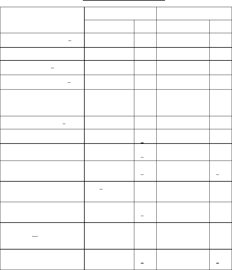
TABLE I. Class level S and level B screening
.
Screen
Class level S Class level B
Method Reqt Method Reqt
3.1.1 Wafer lot acceptance 1/ 5007 All
lots
---
3.1.2 Nondestructive bond pull 2023 100%
---
3.1.3 Internal visual 2/ 2010, test
condition A
100% 2010, test
condition B
100%
3.1.4 Temperature cycling 3/ 1010, test
condition C
100% 1010, test
condition C
100%
3.1.5 Constant acceleration
(see 3.2 and 3.4.2)
2001, test
condition E
(min) Y1
orientation only
100% 2001, test
condition E
(min) Y1
orientation only
100%
3.1.6 Visual inspection 4/
100%
100%
3.1.7 Particle impact noise
detection (PIND)
2020, test
condition A
100%
5
/
---
3.1.8 Serialization
100%
6
/
---
3.1.9 Pre burn-in electrical
parameters (see 3.5.1)
In accordance with
applicable device
specification
100%
7
/
In accordance with
applicable device
specification
100%
8
/
3.1.10 Burn-in test (see 3.4.2) 1015 9/
240 hours at
125°C minimum
100% 1015
160 hours at 125°C
minimum
100%
3.1.11 Interim (post burn-in)
electrical parameters (see 3.5.1)
In accordance with
applicable device
specification
100%
7
/
---
3.1.12 Reverse bias burn-in
(see 3.4.2) 10
/
1015; test
condition A or C,
72 hours at 150°C
minimum
100%
---
3.1.13 Interim (post burn-in)
electrical parameters (see 3.5.1)
In accordance with
applicable device
specification
100%
7
/
In accordance with
applicable device
specification
100%
8
/
See footnotes at end of table.
MIL-STD-883F
METHOD 5004.11
18 June 2004
4
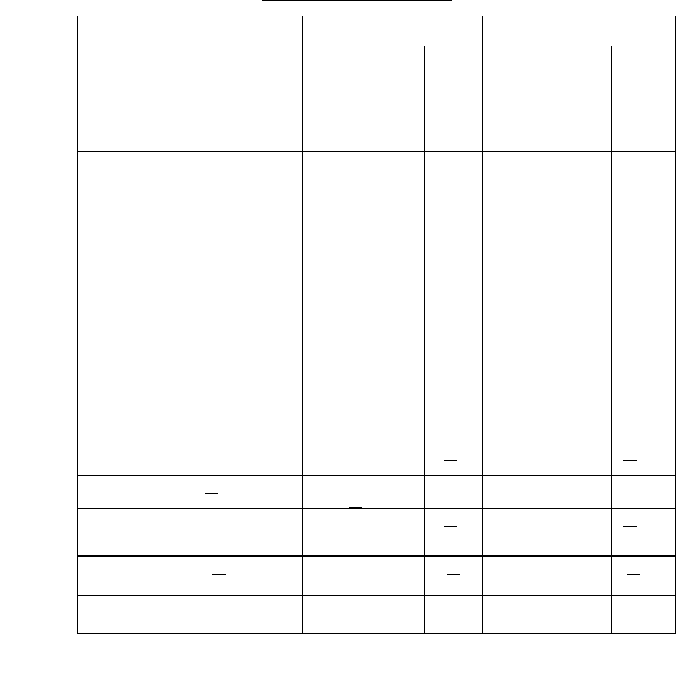
TABLE I. Class level S and level B screening
- Continued.
Screen
Class level S Class level B
Method Reqt Method Reqt
3.1.14 Percent defective
allowable (PDA) calculation
5 percent, see
3.5.1, 3 percent,
functional
parameters at
25°C
All
lots
5 percent, see 3.5.1 All
lots
3.1.15 Final electrical test
(see 3.5.2)
a. Static tests
(1) 25°C (subgroup 1, table I,
5005)
(2) Maximum and minimum rated
operating temperature
(subgroups 2, 3, table I,
5005)
b. Dynamic or functional tests 11
/
(1) 25°C (subgroup 4 or 7,
table I method 5005)
(2) Minimum and maximum rated
operating temperature
(subgroups 5 and 6, or 8
table I method 5005)
c. Switching tests at 25°C
(subgroup 9, table I,
method 5005)
In accordance with
applicable device
specification
100%
100`%
100%
100%
100%
In accordance with
applicable device
specification
100%
100%
100%
100%
100%
3.1.16 Seal
a. Fine
b. Gross
1014 100%
12
/
1014 100%
12
/
3.1.17 Radiographic 13/ 2012 two
views 14
/
100%
---
3.1.18 Qualification or quality
conformance inspection test sample
selection
15/
15/
3.1.19 External visual 16/
2009 17/ 2009 17/
3.1.20 Radiation latch-up
(see 3.5.3) 18
/
1020 100% 1020 100%
See footnotes on next two pages.
*

MIL-STD-883F
METHOD 5004.11
18 June 2004
5
TABLE I. Class level S and level B screening
- Continued.
1
/ All lots shall be selected for testing in accordance with the requirements of method 5007 herein.
2
/ Unless otherwise specified, at the manufacturer's option, test samples for group B, bond strength (method 5005) may
be randomly selected prior to or following internal visual (method 5004), prior to sealing provided all other specification
requirements are satisfied (e.g., bond strength requirements shall apply to each inspection lot, bond failures shall be
counted even if the bond would have failed internal visual exam). Test method 2010 applies in full except when
method 5004, alternate 1 or alternate 2 (appendix A) is in effect (see 3.3).
3
/ For class level B devices, this test may be replaced with thermal shock method 1011, test condition A, minimum.
4
/ At the manufacturer's option, visual inspection for catastrophic failures may be conducted after each of the
thermal/mechanical screens, after the sequence or after seal test. Catastrophic failures are defined as missing leads,
broken packages, or lids off.
5
/ See appendix A of MIL-PRF-38535, A.4.6.3. The PIND test may be performed in any sequence after 3.1.4 and prior to
3.1.13.
6
/ Class level S devices shall be serialized prior to initial electrical parameter measurements.
7
/ Post burn-in electrical parameters shall be read and recorded (see 3.1.13, subgroup 1). Pre burn-in or interim
electrical parameters (see 3.1.9 and 3.1.11) shall be read and recorded only when delta measurements have been
specified as part of post burn-in electrical measurements.
8
/ When specified in the applicable device specification, 100 percent of the devices shall be tested for those parameters
requiring delta calculations.
9
/ Dynamic burn-in only. Test condition F of method 1015 and 3.4.2 herein shall not apply.
10
/ The reverse bias burn-in (see 3.1.12) is a requirement only when specified in the applicable device specification and is
recommended only for a certain MOS, linear or other microcircuits where surface sensitivity may be of concern. When
reverse bias burn-in is not required, interim electrical parameter measurements 3.1.11 are omitted. The order of
performing the burn-in (see 3.1.10) and the reverse bias burn-in may be inverted.
11
/ Functional tests shall be conducted at input test conditions as follows:
V
IH
= V
IH
(min) +20 percent, -0 percent; V
IL
= V
IL
(max) +0 percent, -50 percent; as specified in the most similar military
detail specification. Devices may be tested using any input voltage within this input voltage range but shall be
guaranteed to V
IH
(min) and V
IL
(max).
CAUTION: To avoid test correlation problems, the test system noise (e.g., testers, handlers, etc.) should be verified
to assure that V
IH
(min) and V
IL
(max) requirements are not violated at the device terminals.
*