MIL- STD-883F 2004 TEST METHOD STANDARD MICROCIRCUITS.pdf - 第595页
MIL-STD-883F METHOD 5004.11 18 June 2004 5 TABLE I. Clas s l evel S and level B s creeni ng - Conti nued. 1 / Al l lot s shal l be sel ected f or tes ting in ac cor dance wit h the requir ements of method 5007 herei n. 2…
MIL-STD-883F
METHOD 5004.11
18 June 2004
4
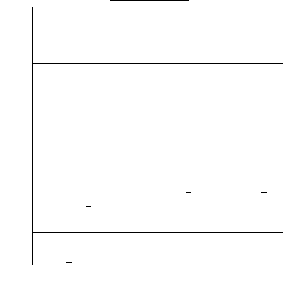
TABLE I. Class level S and level B screening
- Continued.
Screen
Class level S Class level B
Method Reqt Method Reqt
3.1.14 Percent defective
allowable (PDA) calculation
5 percent, see
3.5.1, 3 percent,
functional
parameters at
25°C
All
lots
5 percent, see 3.5.1 All
lots
3.1.15 Final electrical test
(see 3.5.2)
a. Static tests
(1) 25°C (subgroup 1, table I,
5005)
(2) Maximum and minimum rated
operating temperature
(subgroups 2, 3, table I,
5005)
b. Dynamic or functional tests 11
/
(1) 25°C (subgroup 4 or 7,
table I method 5005)
(2) Minimum and maximum rated
operating temperature
(subgroups 5 and 6, or 8
table I method 5005)
c. Switching tests at 25°C
(subgroup 9, table I,
method 5005)
In accordance with
applicable device
specification
100%
100`%
100%
100%
100%
In accordance with
applicable device
specification
100%
100%
100%
100%
100%
3.1.16 Seal
a. Fine
b. Gross
1014 100%
12
/
1014 100%
12
/
3.1.17 Radiographic 13/ 2012 two
views 14
/
100%
---
3.1.18 Qualification or quality
conformance inspection test sample
selection
15/
15/
3.1.19 External visual 16/
2009 17/ 2009 17/
3.1.20 Radiation latch-up
(see 3.5.3) 18
/
1020 100% 1020 100%
See footnotes on next two pages.
*

MIL-STD-883F
METHOD 5004.11
18 June 2004
5
TABLE I. Class level S and level B screening
- Continued.
1
/ All lots shall be selected for testing in accordance with the requirements of method 5007 herein.
2
/ Unless otherwise specified, at the manufacturer's option, test samples for group B, bond strength (method 5005) may
be randomly selected prior to or following internal visual (method 5004), prior to sealing provided all other specification
requirements are satisfied (e.g., bond strength requirements shall apply to each inspection lot, bond failures shall be
counted even if the bond would have failed internal visual exam). Test method 2010 applies in full except when
method 5004, alternate 1 or alternate 2 (appendix A) is in effect (see 3.3).
3
/ For class level B devices, this test may be replaced with thermal shock method 1011, test condition A, minimum.
4
/ At the manufacturer's option, visual inspection for catastrophic failures may be conducted after each of the
thermal/mechanical screens, after the sequence or after seal test. Catastrophic failures are defined as missing leads,
broken packages, or lids off.
5
/ See appendix A of MIL-PRF-38535, A.4.6.3. The PIND test may be performed in any sequence after 3.1.4 and prior to
3.1.13.
6
/ Class level S devices shall be serialized prior to initial electrical parameter measurements.
7
/ Post burn-in electrical parameters shall be read and recorded (see 3.1.13, subgroup 1). Pre burn-in or interim
electrical parameters (see 3.1.9 and 3.1.11) shall be read and recorded only when delta measurements have been
specified as part of post burn-in electrical measurements.
8
/ When specified in the applicable device specification, 100 percent of the devices shall be tested for those parameters
requiring delta calculations.
9
/ Dynamic burn-in only. Test condition F of method 1015 and 3.4.2 herein shall not apply.
10
/ The reverse bias burn-in (see 3.1.12) is a requirement only when specified in the applicable device specification and is
recommended only for a certain MOS, linear or other microcircuits where surface sensitivity may be of concern. When
reverse bias burn-in is not required, interim electrical parameter measurements 3.1.11 are omitted. The order of
performing the burn-in (see 3.1.10) and the reverse bias burn-in may be inverted.
11
/ Functional tests shall be conducted at input test conditions as follows:
V
IH
= V
IH
(min) +20 percent, -0 percent; V
IL
= V
IL
(max) +0 percent, -50 percent; as specified in the most similar military
detail specification. Devices may be tested using any input voltage within this input voltage range but shall be
guaranteed to V
IH
(min) and V
IL
(max).
CAUTION: To avoid test correlation problems, the test system noise (e.g., testers, handlers, etc.) should be verified
to assure that V
IH
(min) and V
IL
(max) requirements are not violated at the device terminals.
*

MIL-STD-883F
METHOD 5004.11
18 June 2004
6
TABLE I. Class level S and level B screening
- Continued.
12
/ For class level B devices, the fine and gross seal tests (3.1.16) shall be performed separately or together, between
constant acceleration (3.1.5) and external visual (3.1.19). For class level S devices, the fine and gross seal tests
(3.1.16) shall be performed separately or together, between final electrical testing (3.1.15) and external visual (3.1.19).
In addition, for class level S and level B devices, all device lots (sublots) having any physical processing steps (e.g.,
lead shearing, lead forming, solder dipping to the glass seal, change of, or rework to, the lead finish, etc.) performed
following seal (3.1.16) or external visual (3.1.19) shall be retested for hermeticity and visual defects. This shall be
accomplished by performing, and passing, as a minimum, a sample seal test (method 1014) using an acceptance
criteria of a quantity (accept number) of 116(0), and an external visual inspection (method 2009) on the entire
inspection lot (sublot). For devices with leads that are not glass-sealed and that have a lead pitch less than or equal
to 1.27 mm (0.050 inch), the sample seal test shall be performed using an acceptance criteria of a quantity (accept
number) of 15(0). If the sample fails the acceptance criteria specified, all devices in the inspection lot represented by
the sample shall be subjected to the fine and gross seal tests and all devices that fail shall be removed from the lot for
final acceptance. For class level S devices, with the approval of the qualifying activity, an additional room temperature
electrical test may be performed subsequent to seal (3.1.16), but before external visual (3.1.19) if the devices are
installed in individual carriers during electrical test.
13
/ The radiographic (see 3.1.17) screen may be performed in any sequence after 3.1.8.
14
/ Only one view is required for flat packages and leadless chip carriers having lead (terminal) metal on four sides.
15
/ Samples shall be selected for testing in accordance with the specific device class and lot requirements of method
5005. See 3.5 of method 5005.
16
/ External visual shall be performed on the lot any time after 3.1.17 and prior to shipment, and all shippable samples
shall have external visual inspection at least subsequent to qualification or quality conformance inspection testing.
17
/ The manufacturer shall inspect the devices 100 percent or on a sample basis using a quantity/accept number of
116(0). If one or more rejects occur in this sample, the manufacturer may double the sample size with no additional
failures allowed or inspect the remaining devices 100 percent for the failed criteria and remove the failed devices from
the lot. If the double sample also has one or more failures, the manufacturer shall be required to 100 percent inspect
the remaining devices in the lot for the failed criteria. Reinspection magnification shall be no less than that used for
the original inspection for the failed criteria.
18
/ Radiation latch-up screen shall be conducted when specified in purchase order or contract. Latch-up screen is not
required for SOS, SOI, and DI technology when latch-up is physically not possible. At the manufacturer's option,
latch-up screen may be conducted at any screening operation step after seal.
3.3.2 Description of special electrical screening tests
. The special electrical screens shall consist of a series of electrical
tests each of which can be categorized as either a voltage stress test or a low level leakage test.
3.3.2.1 Voltage stress tests
. The purpose of voltage stress tests is to eliminate those failure mechanisms which are
voltage sensitive. These tests shall be designed such that each circuit element (including metallization runs) within the
microcircuit is stressed by an applied voltage which approaches or exceeds (under current limited conditions) the breakdown
voltage of the circuit element under test. For those elements which cannot be placed in a reverse bias mode, the applied
voltage must be equal to or greater than 120 percent of the normal operating voltage. Any device which exhibits abnormal
leakage currents at the specified applied voltage conditions shall be rejected. The number of stress tests being performed
will vary from a few for a simple gate to many for MSI or LSI functions.