MIL- STD-883F 2004 TEST METHOD STANDARD MICROCIRCUITS.pdf - 第653页
MIL-STD-883F METHOD 5010.4 18 June 2004 3 TAB LE II. P ack age eval uation requi rement s . Subgroup Class le vels Test MI L-STD-883 Quantit y (acc ept number) Referenc e paragrap h S B Method Condit ion 1 X X Phys ic al…
MIL-STD-883F
METHOD 5010.4
18 June 2004
2
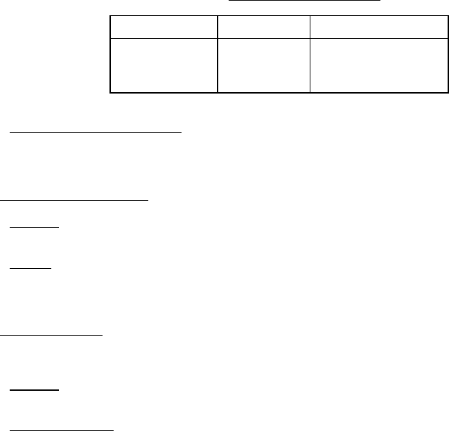
TABLE I. Element evaluation summary.
Element Paragraph Requirement
Microcircuit wafer 3.2.2 Appendix II (herein)
Package 3.2.3 Table II (herein)
3.2.1.2 Element evaluation requirements
. Element evaluation may be performed at either the element supplier or device
manufacturing facility up to the point where the element must undergo processing or assembly prior to testing. If element
evaluation is performed by the supplier, then the device manufacturer must obtain a summary of the results for verification,
and record retention.
3.2.2 Microcircuit wafer evaluation
.
3.2.2.1 Definition
. Diffused wafers used and evaluated shall, as a minimum, be complete with interconnect layers and
glassivation from material that was homogeneously processed through wafer fabrication.
3.2.2.2 General
. For the purpose of microcircuit wafer evaluation and wafer lot acceptance, measurement of the process
monitor (PM), verifying that the identified parameters are within process limits, will be required from each wafer lot in
accordance with appendix II wafer lot acceptance herein. Each die from each diffused wafer lot shall be electrically tested
prior to assembly in accordance with the manufacturer's in-house documentation.
3.2.3 Package evaluation
. Each package type shall be evaluated and characterized in accordance with table II herein
prior to use. Finite element analyses techniques may be used. Packages used for complex monolithic microcircuits and
fabricated to this test method shall be tested as follows:
3.2.3.1 Definition
. Package used and evaluated shall consist of the same element specifications, materials, and finish;
and homogeneously processed through device assembly.
3.2.3.2 Incoming inspection
.
a. From the initial package inspection lot, a randomly selected sample shall be subjected to package evaluation (see
table II). Additionally, subgroup 3 testing shall be accomplished using sealed packages. A die may be attached.
Subgroups 2, 3, and 4 apply to cases only.
b. Additionally, subgroups 1, 2, and 3 of table II shall be accomplished for each subsequent acquisition.
c. For solderability (subgroup 2), lead integrity (subgroup 3), and metal package isolation (subgroup 4) defined within
table II, a quantity (accept number) of 15 (0) shall apply to the number of terminals or leads tested. The leads
shall be randomly selected from the three packages.
MIL-STD-883F
METHOD 5010.4
18 June 2004
3
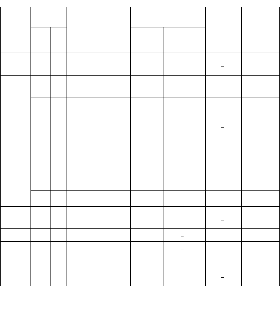
TABLE II. Package evaluation requirements
.
Subgroup
Class levels
Test MIL-STD-883 Quantity
(accept
number)
Reference
paragraph
S B
Method Condition
1 X X Physical dimensions 2016
15 (0) 3.2.3.3
2 X X Solderability 2003 Solderability
temperature
245 ±5°C
3 (0)
1
/
3 X X Thermal shock
or
Temperature cycle
1011
1010
C
C (20 cycles)
3 (0)
X X High temperature bake 1008 2 hours at
150°C
3 (0)
X X Lead integrity 2004
2028
B2
(lead fatigue)
D
(leadless chip
carriers)
B1
(leaded chip
carrier
packages)
(Pin grid array
leads and
rigid leads)
3 (0)
1
/
X X Seal 1014 D
Sealed cases
3 (0)
4 X X Metal package
isolation
1003 600 V dc,
100 nA
maximum
3 (0)
1
/
3.2.3.4
5 X X Insulation 1003 2/ 3 (0)
6 X X Conductor MIL-STD-
202
method
307
2/ 3 (0)
7 X X Thermal
characterization
1012
3/
1
/ A quantity (accept number) of 15 (0) shall apply to the number of terminals or leads to be tested. The leads
shall be randomly selected from three packages minimum.
2
/ Selected from three packages minimum. Conditions as specified by acquisition document and Appendix A of
MIL-PRF-38535.
3
/ Required on all package types prior to initial use.

MIL-STD-883F
METHOD 5010.4
18 June 2004
4
3.2.3.3 Subgroup 1. Separately verify case and cover dimensional compliance with the device specification or drawing.
3.2.3.4 Subgroup 4
. For metal cases with leads separated by an insulator, measure insulation resistance between the
metal body of the case and the leads that are isolated from the case. This test does not apply to nonmetallic cases.
3.3 Manufacturing control
.
3.3.1 Process control requirements
. Line control as detailed below is required.
3.3.1.1 Wafer fabrication controls
. Wafer fabrication shall be controlled in accordance with the manufacturer's fabrication
baseline and documented procedures of the fabrication process.
3.3.1.2 Assembly controls
. Assembly controls shall be in accordance with the manufacturer's assembly baseline and
documented assembly procedures and additions herein
3.3.2 Design/layout system control
. Design/layout controls shall be implemented using appendix I as a guide.
3.3.3 Testing controls
. Documentation of testing controls shall meet the requirements of MIL-PRF-38535, appendix A.
3.3.3.1 Test vectors
. The manufacturing-level logic test vectors shall be graded for fault coverage using a fault simulator.
The resulting fault coverage shall be reported in the device specification or drawing. Fault coverage shall be based on the
detectable equivalence classes of single, permanent, stuck at zero, and stuck at one faults on all logic lines of a structural
logic model. The logic model shall be expressed in terms of gate-level primitives or simple atomic functions (such as
flip-flops). Large, regular structures such as RAMs and ROMs shall not be modeled at the gate level; rather, documentation
shall be provided to show that these structures are tested using appropriate procedures (such as, galloping patterns for a
RAM).
3.3.3.2 Built-in-test/build-in-redundancy
. When specified in the device specification or drawing, the following shall apply.
3.3.3.2.1 Probe/bond sites
. The device shall contain probe/bond sites to allow testing using the full set of test vectors
specified in the device specification or drawing.
3.3.3.2.2 Built-in redundancy for yield enhancement
. Where built-in redundancy is used to provide yield enhancement,
testing shall be included to provide a statistic which represents the amount of alternate element selection utilized.
3.3.3.2.3 Built-in redundancy using self test and fix
. Where built-in redundancy is provided in the form of self test and fix,
the circuitry will be capable of interrogation to determine the level of redundancy remaining on the device.
3.3.4 Quality controls
. The product assurance program plan shall be in accordance with MIL-PRF-38535, appendix A.
3.3.4.1 Process monitor
. Process control and stability of dc parameters must be demonstrated through the use of the
manufacturer's process monitor (PM). The PM is to be designed so that the dc process parameters may be measured in
wafer form. The PM may also be packaged so as to permit biasing of those circuits for measurement. The PM design must
be submitted to the qualifying activity for approval prior to qualification and must contain as a minimum the structures
outlined in table I of appendix II herein.
*