MIL- STD-883F 2004 TEST METHOD STANDARD MICROCIRCUITS.pdf - 第655页
MIL-STD-883F METHOD 5010.4 18 June 2004 5 3.3.4. 1.1 Proc ess moni tors f or other tec hnology de vic es . An adequate s et of PM' s appli cable for other t echnology devices shall be generate d to ass ure t hat app…

MIL-STD-883F
METHOD 5010.4
18 June 2004
4
3.2.3.3 Subgroup 1. Separately verify case and cover dimensional compliance with the device specification or drawing.
3.2.3.4 Subgroup 4
. For metal cases with leads separated by an insulator, measure insulation resistance between the
metal body of the case and the leads that are isolated from the case. This test does not apply to nonmetallic cases.
3.3 Manufacturing control
.
3.3.1 Process control requirements
. Line control as detailed below is required.
3.3.1.1 Wafer fabrication controls
. Wafer fabrication shall be controlled in accordance with the manufacturer's fabrication
baseline and documented procedures of the fabrication process.
3.3.1.2 Assembly controls
. Assembly controls shall be in accordance with the manufacturer's assembly baseline and
documented assembly procedures and additions herein
3.3.2 Design/layout system control
. Design/layout controls shall be implemented using appendix I as a guide.
3.3.3 Testing controls
. Documentation of testing controls shall meet the requirements of MIL-PRF-38535, appendix A.
3.3.3.1 Test vectors
. The manufacturing-level logic test vectors shall be graded for fault coverage using a fault simulator.
The resulting fault coverage shall be reported in the device specification or drawing. Fault coverage shall be based on the
detectable equivalence classes of single, permanent, stuck at zero, and stuck at one faults on all logic lines of a structural
logic model. The logic model shall be expressed in terms of gate-level primitives or simple atomic functions (such as
flip-flops). Large, regular structures such as RAMs and ROMs shall not be modeled at the gate level; rather, documentation
shall be provided to show that these structures are tested using appropriate procedures (such as, galloping patterns for a
RAM).
3.3.3.2 Built-in-test/build-in-redundancy
. When specified in the device specification or drawing, the following shall apply.
3.3.3.2.1 Probe/bond sites
. The device shall contain probe/bond sites to allow testing using the full set of test vectors
specified in the device specification or drawing.
3.3.3.2.2 Built-in redundancy for yield enhancement
. Where built-in redundancy is used to provide yield enhancement,
testing shall be included to provide a statistic which represents the amount of alternate element selection utilized.
3.3.3.2.3 Built-in redundancy using self test and fix
. Where built-in redundancy is provided in the form of self test and fix,
the circuitry will be capable of interrogation to determine the level of redundancy remaining on the device.
3.3.4 Quality controls
. The product assurance program plan shall be in accordance with MIL-PRF-38535, appendix A.
3.3.4.1 Process monitor
. Process control and stability of dc parameters must be demonstrated through the use of the
manufacturer's process monitor (PM). The PM is to be designed so that the dc process parameters may be measured in
wafer form. The PM may also be packaged so as to permit biasing of those circuits for measurement. The PM design must
be submitted to the qualifying activity for approval prior to qualification and must contain as a minimum the structures
outlined in table I of appendix II herein.
*

MIL-STD-883F
METHOD 5010.4
18 June 2004
5
3.3.4.1.1 Process monitors for other technology devices
. An adequate set of PM's applicable for other technology
devices shall be generated to assure that applicable failure mechanisms are detected and submitted for approval by the
qualifying activity.
3.3.4.2 Qualification device
. A qualification device shall be used to demonstrate process stability and reliability. The
qualification device, either a standard evaluation circuit (SEC) or an actual device (worst case design) shall be submitted to
the qualifying activity for approval and as such contain the basic information as detailed herein. The qualification device
shall be fabricated with the same process and designed to the same design rules that will produce any device in the
technology to be qualified. The qualification device design shall be configured in such a manner so as to evaluate the
reliability of the underlayer designs (e.g., diffusion) and evaluate the worst case design rule conditions on the personalization
layers. The design should utilize cell libraries as well as test structures which will detect metal to metal shorting or opening,
high via resistance and dielectric pinholes during reliability life testing, where applicable. The following structures are
suggested:
Parameter
Structure
Functionality and performance Large functional block (ALU),
ring oscillator
Contact resistance/electromigration Contact strings
Hot electrons/holes Short channel devices
Oxide breakdown voltage Capacitors
Resistance (electromigration test) Metal stripes
3.4 Screening procedures for microcircuits
. Screening of microcircuits shall be conducted as described in 3.4 through
3.4.13 and table III herein. This provision does not preclude the performance of additional tests or inspection which may be
required for specific devices or which may be desirable to optimize results of screening; however, any such special test
inspection shall be subjected to the requirements of appendix A of MIL-PRF-38535, A.4.3.4 and A.4.3.7. Sampling
inspections shall not be an acceptable substitute for any specified screening test. Any burn-in, in addition to that specified,
is only permitted when documented in the lot records, and any failures shall be counted in applicable PDA calculations.
Where end point or post test measurements are required as part of any given test method used in the screening procedure
and where such post-test measurements are duplicated in the interim (post burn-in) or final electrical tests that follow, such
measurements need not be duplicated and need to be performed only as part of the interim (post burn-in) or final electrical
tests. Devices which pass screening requirements of a higher reliability level shall be considered to meet the screening
requirements of all lower levels. In no case shall screening to a lower level than that specified be permitted.
3.4.1 General
.
a. Devices that fail any test or inspection criteria in the screening sequence shall be removed from the lot at the time
of observation or immediately at the conclusion of the test in which the failure was observed. Once rejected and
verified as a device failure, no device may be retested for acceptance. Unless otherwise specified in the device
specification or drawings, electrical rejects may be used to satisfy sample selection requirements for qualification
and quality conformance inspection in accordance with 3.5.
b. Device screening shall be performed in the sequence shown in table III except where variations in sequence are
specifically allowed herein.
*
MIL-STD-883F
METHOD 5010.4
18 June 2004
6
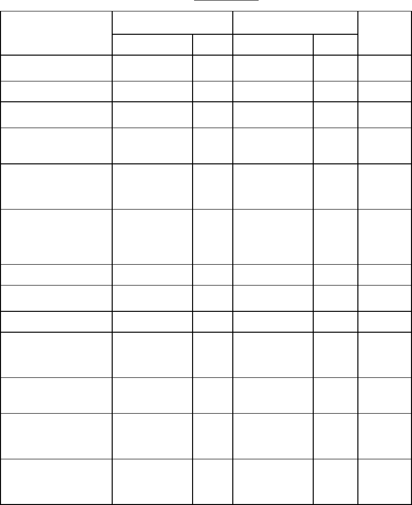
TABLE III. Device screening.
Screen
Class level S Class level B Reference
paragraph
Method Reqmt Method Reqmt
Wafer lot acceptance 5010 appendix II
and 5007
All
lots
5010 appendix II All
lots
Nondestructive bond pull 2023 100%
Internal visual 2010, test
condition A
100% 2010, test
condition B
100% 3.4.2
Stabilization bake. No
end point measurements
required
3.4.3
Temperature cycling or
thermal shock
1010, test
condition C
100% 1010, test
condition C
1011, test
condition A
100%
100%
3.4.5
Constant acceleration 2001, test
condition E
(min) Y1
orientation
only
100% 2001, test
condition E
(min) Y1
orientation
only
100% 3.4.6
Visual inspection
100%
100%
Particle impact noise
detection (PIND)
2020, test
condition A
100%
3.4.7
Serialization
100%
Interim (pre-burn-in)
electrical parameters
In accordance
with applicable
device
specification
100% In accordance
with applicable
device
specification
100% 3.4.9.1
Burn-in test 1015
240 hours at
125°C minimum
100% 1015
160 hours at
125°C minimum
100% 3.4.10
Interim (post-burn-in)
electrical parameters
In accordance
with applicable
device
specification
100%
Optional
3.4.9.1
Reverse bias burn-in 1015; test
condition A or
C, 72 hours at
150° minimum.
100%