MIL- STD-883F 2004 TEST METHOD STANDARD MICROCIRCUITS.pdf - 第656页
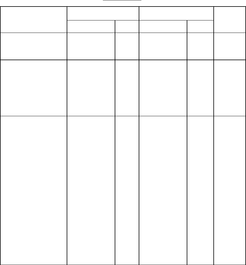
MIL-STD-883F METHOD 5010.4 18 June 2004 6 TABL E III. Dev ice scr eening . Screen Class lev el S Class lev el B Refer ence paragra ph Method Reqmt Method Reqmt W afer lot accept ance 5010 appen dix II and 5007 All lots 5…

MIL-STD-883F
METHOD 5010.4
18 June 2004
5
3.3.4.1.1 Process monitors for other technology devices
. An adequate set of PM's applicable for other technology
devices shall be generated to assure that applicable failure mechanisms are detected and submitted for approval by the
qualifying activity.
3.3.4.2 Qualification device
. A qualification device shall be used to demonstrate process stability and reliability. The
qualification device, either a standard evaluation circuit (SEC) or an actual device (worst case design) shall be submitted to
the qualifying activity for approval and as such contain the basic information as detailed herein. The qualification device
shall be fabricated with the same process and designed to the same design rules that will produce any device in the
technology to be qualified. The qualification device design shall be configured in such a manner so as to evaluate the
reliability of the underlayer designs (e.g., diffusion) and evaluate the worst case design rule conditions on the personalization
layers. The design should utilize cell libraries as well as test structures which will detect metal to metal shorting or opening,
high via resistance and dielectric pinholes during reliability life testing, where applicable. The following structures are
suggested:
Parameter
Structure
Functionality and performance Large functional block (ALU),
ring oscillator
Contact resistance/electromigration Contact strings
Hot electrons/holes Short channel devices
Oxide breakdown voltage Capacitors
Resistance (electromigration test) Metal stripes
3.4 Screening procedures for microcircuits
. Screening of microcircuits shall be conducted as described in 3.4 through
3.4.13 and table III herein. This provision does not preclude the performance of additional tests or inspection which may be
required for specific devices or which may be desirable to optimize results of screening; however, any such special test
inspection shall be subjected to the requirements of appendix A of MIL-PRF-38535, A.4.3.4 and A.4.3.7. Sampling
inspections shall not be an acceptable substitute for any specified screening test. Any burn-in, in addition to that specified,
is only permitted when documented in the lot records, and any failures shall be counted in applicable PDA calculations.
Where end point or post test measurements are required as part of any given test method used in the screening procedure
and where such post-test measurements are duplicated in the interim (post burn-in) or final electrical tests that follow, such
measurements need not be duplicated and need to be performed only as part of the interim (post burn-in) or final electrical
tests. Devices which pass screening requirements of a higher reliability level shall be considered to meet the screening
requirements of all lower levels. In no case shall screening to a lower level than that specified be permitted.
3.4.1 General
.
a. Devices that fail any test or inspection criteria in the screening sequence shall be removed from the lot at the time
of observation or immediately at the conclusion of the test in which the failure was observed. Once rejected and
verified as a device failure, no device may be retested for acceptance. Unless otherwise specified in the device
specification or drawings, electrical rejects may be used to satisfy sample selection requirements for qualification
and quality conformance inspection in accordance with 3.5.
b. Device screening shall be performed in the sequence shown in table III except where variations in sequence are
specifically allowed herein.
*

MIL-STD-883F
METHOD 5010.4
18 June 2004
6
TABLE III. Device screening.
Screen
Class level S Class level B Reference
paragraph
Method Reqmt Method Reqmt
Wafer lot acceptance 5010 appendix II
and 5007
All
lots
5010 appendix II All
lots
Nondestructive bond pull 2023 100%
Internal visual 2010, test
condition A
100% 2010, test
condition B
100% 3.4.2
Stabilization bake. No
end point measurements
required
3.4.3
Temperature cycling or
thermal shock
1010, test
condition C
100% 1010, test
condition C
1011, test
condition A
100%
100%
3.4.5
Constant acceleration 2001, test
condition E
(min) Y1
orientation
only
100% 2001, test
condition E
(min) Y1
orientation
only
100% 3.4.6
Visual inspection
100%
100%
Particle impact noise
detection (PIND)
2020, test
condition A
100%
3.4.7
Serialization
100%
Interim (pre-burn-in)
electrical parameters
In accordance
with applicable
device
specification
100% In accordance
with applicable
device
specification
100% 3.4.9.1
Burn-in test 1015
240 hours at
125°C minimum
100% 1015
160 hours at
125°C minimum
100% 3.4.10
Interim (post-burn-in)
electrical parameters
In accordance
with applicable
device
specification
100%
Optional
3.4.9.1
Reverse bias burn-in 1015; test
condition A or
C, 72 hours at
150° minimum.
100%
MIL-STD-883F
METHOD 5010.4
18 June 2004
7
TABLE III. Device screening -Continued.
Screen
Class level S Class level B Reference
paragraph
Method Reqmt. Method Reqmt.
Interim (post-burn-in)
electrical parameters
In accordance
with applicable
device
specification
100% In accordance
with applicable
device
specification
100% 3.4.9.1
Percent defective
allowable (PDA)
calculation
5 percent
(subgroup 1,
table IV)
3 percent
functional
parameters at
25°C
(subgroup 7
table IV)
All
lots
5 percent
(subgroup 1,
table IV)
All
lots
3.4.9.1
Final electrical test
a. Static tests
(1) 25°C (subgroup 1,
table IV)
(2) Maximum and
minimum rated
operating temp.
(subgroup 2, 3,
(table IV)
b. Dynamic or functional
tests
(1) 25°C (subgroup 4,
or 7, table IV)
(2) Minimum and
maximum rated
operating temp.
(subgroup 5 and
6, or 8, table
IV)
c. Switching tests at
25°C (subgroup 9,)
table IV)
In accordance
with applicable
device
specification
100%
100%
100%
100%
100%
In accordance
with applicable
device
specification
100%
100%
100%
100%
100%
3.4.11