MIL- STD-883F 2004 TEST METHOD STANDARD MICROCIRCUITS.pdf - 第657页
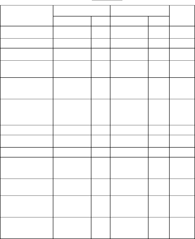
MIL-STD-883F METHOD 5010.4 18 June 2004 7 TABL E III. Dev ice scr eening -Conti nued. S creen C lass leve l S C lass leve l B Referenc e paragra ph Me thod Reqmt. Metho d Reqmt . Inter im (pos t-burn- in) elect rical par…
MIL-STD-883F
METHOD 5010.4
18 June 2004
6
TABLE III. Device screening.
Screen
Class level S Class level B Reference
paragraph
Method Reqmt Method Reqmt
Wafer lot acceptance 5010 appendix II
and 5007
All
lots
5010 appendix II All
lots
Nondestructive bond pull 2023 100%
Internal visual 2010, test
condition A
100% 2010, test
condition B
100% 3.4.2
Stabilization bake. No
end point measurements
required
3.4.3
Temperature cycling or
thermal shock
1010, test
condition C
100% 1010, test
condition C
1011, test
condition A
100%
100%
3.4.5
Constant acceleration 2001, test
condition E
(min) Y1
orientation
only
100% 2001, test
condition E
(min) Y1
orientation
only
100% 3.4.6
Visual inspection
100%
100%
Particle impact noise
detection (PIND)
2020, test
condition A
100%
3.4.7
Serialization
100%
Interim (pre-burn-in)
electrical parameters
In accordance
with applicable
device
specification
100% In accordance
with applicable
device
specification
100% 3.4.9.1
Burn-in test 1015
240 hours at
125°C minimum
100% 1015
160 hours at
125°C minimum
100% 3.4.10
Interim (post-burn-in)
electrical parameters
In accordance
with applicable
device
specification
100%
Optional
3.4.9.1
Reverse bias burn-in 1015; test
condition A or
C, 72 hours at
150° minimum.
100%
MIL-STD-883F
METHOD 5010.4
18 June 2004
7
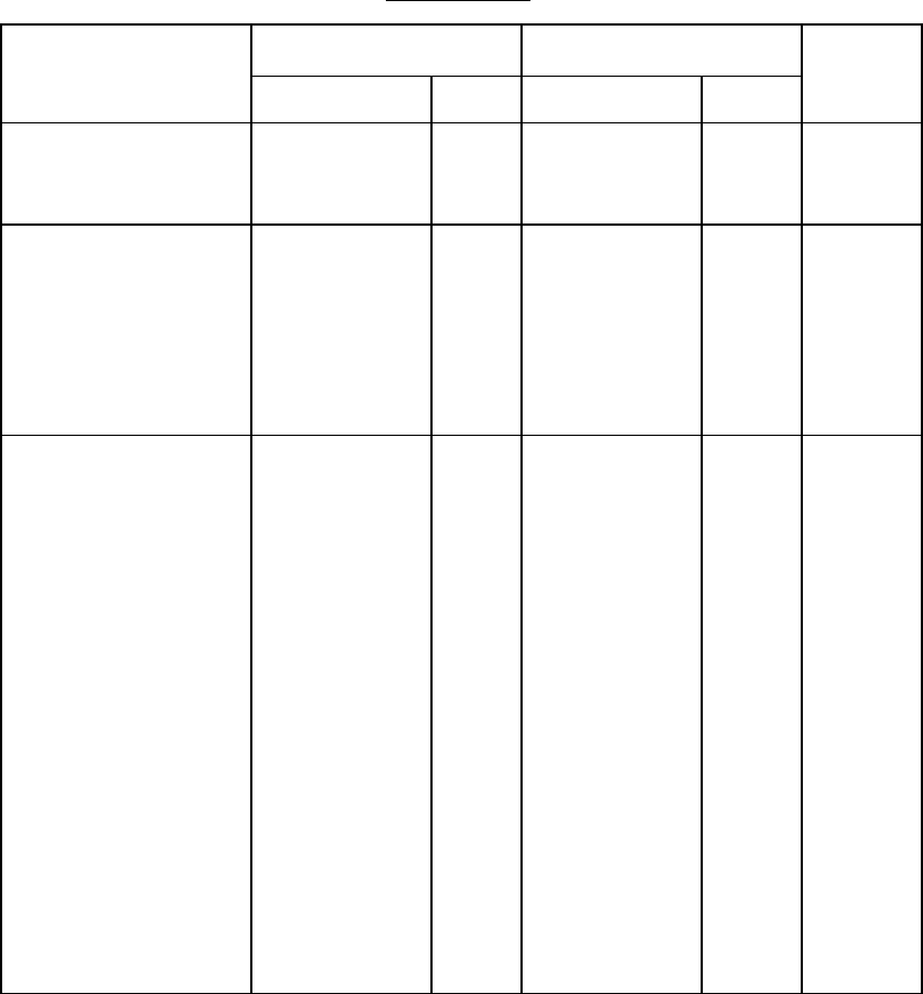
TABLE III. Device screening -Continued.
Screen
Class level S Class level B Reference
paragraph
Method Reqmt. Method Reqmt.
Interim (post-burn-in)
electrical parameters
In accordance
with applicable
device
specification
100% In accordance
with applicable
device
specification
100% 3.4.9.1
Percent defective
allowable (PDA)
calculation
5 percent
(subgroup 1,
table IV)
3 percent
functional
parameters at
25°C
(subgroup 7
table IV)
All
lots
5 percent
(subgroup 1,
table IV)
All
lots
3.4.9.1
Final electrical test
a. Static tests
(1) 25°C (subgroup 1,
table IV)
(2) Maximum and
minimum rated
operating temp.
(subgroup 2, 3,
(table IV)
b. Dynamic or functional
tests
(1) 25°C (subgroup 4,
or 7, table IV)
(2) Minimum and
maximum rated
operating temp.
(subgroup 5 and
6, or 8, table
IV)
c. Switching tests at
25°C (subgroup 9,)
table IV)
In accordance
with applicable
device
specification
100%
100%
100%
100%
100%
In accordance
with applicable
device
specification
100%
100%
100%
100%
100%
3.4.11
MIL-STD-883F
METHOD 5010.4
18 June 2004
8
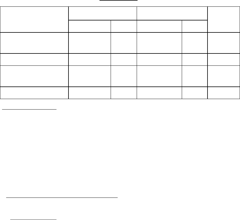
TABLE III. Device screening - Continued.
Screen
Class level S Class level B Reference
paragraph
Method Reqmt. Method Reqmt.
Seal
Fine
Gross
1014 100% 1014 100% 3.4.8
Radiographic 2012 two views 100%
3.4.12
Qualification or quality
conformance inspection
test sample selection
See 3.5
See 3.5
External visual 2009 100% 2009 100% 3.4.13
3.4.2 Internal visual inspection
. Internal visual inspection shall be performed to the requirements of method 2010,
condition A for class level S devices and condition B for class level B devices. Devices awaiting preseal inspection, or other
accepted, unsealed devices awaiting further processing shall be stored in a dry, inert, controlled environment until sealed.
Unless otherwise specified, at the manufacturer's option, test samples for group B, bond strength may be randomly selected
prior to or following internal visual, prior to sealing provided all other specification requirements are satisfied (e.g., bond
strength requirements shall apply to each inspection lot, bond failures shall be counted even if the bond would have failed
internal visual exam).
The alternate procedure of 3.4.2.1 shall be used when any of the following criteria are met:
a. Minimum horizontal geometry is less than three microns.
b. Metallization consists of two or more levels.
c. Opaque materials mask design features.
3.4.2.1 Alternate procedures for class level B microcircuits
. Alternate procedures may be used on an optional basis on
any microcircuit, provided that the conditions and limits of the alternate procedures are submitted to, and approved by the
preparing activity, or the acquiring activity.
3.4.2.1.1 Alternate procedures
. The deletions and the changes stated herein are allowable only if the requirements of
alternate 1 or alternate 2 are met.
Alternate 1: The deletions and the changes stated in 3.4.2.1.1a. are allowable for complex monolithic microcircuits
for class level B product only if the requirements of 3.4.2.1.1.b and 3.4.2.1.1.c are imposed and any
of the following conditions exists.
1. Minimum horizontal geometry is less than 3 micrometers (µm).
2. Interconnects consisting of two or more levels.
3. Opaque materials mask design features.
a. For inspection of each microcircuit die, delete the inspection criteria of 3.1.1, 3.1.2, 3.1.3, 3.1.4, 3.1.5, 3.1.6, 3.1.7,
and 3.2.5 of condition B of method 2010 and for use in conjunction with alternate procedures, add 3.1.1.1, 3.1.1.2,
3.1.1.6, 3.1.3, 3.1.4, and 3.2.5 to the low magnification inspection of method 2010.
b. Temperature cycling (3.4.5). The minimum total number of temperature cycles shall be 50. The manufacturer
may reduce the number of temperature cycles from 50 to the 10 required as part of normal screening based upon
data justifying the reduction in temperature cycles approved by the preparing activity and an approved plan which
shall include the following criteria: