MIL- STD-883F 2004 TEST METHOD STANDARD MICROCIRCUITS.pdf - 第659页
MIL-STD-883F METHOD 5010.4 18 June 2004 9 (1) Reducti on of tes t must be c onsidered s eparat ely for each wafer fabri cati on line and eac h die fam ily. (2) The ma nufac turer shall demonstr ate that t he wafer f abri…
MIL-STD-883F
METHOD 5010.4
18 June 2004
8
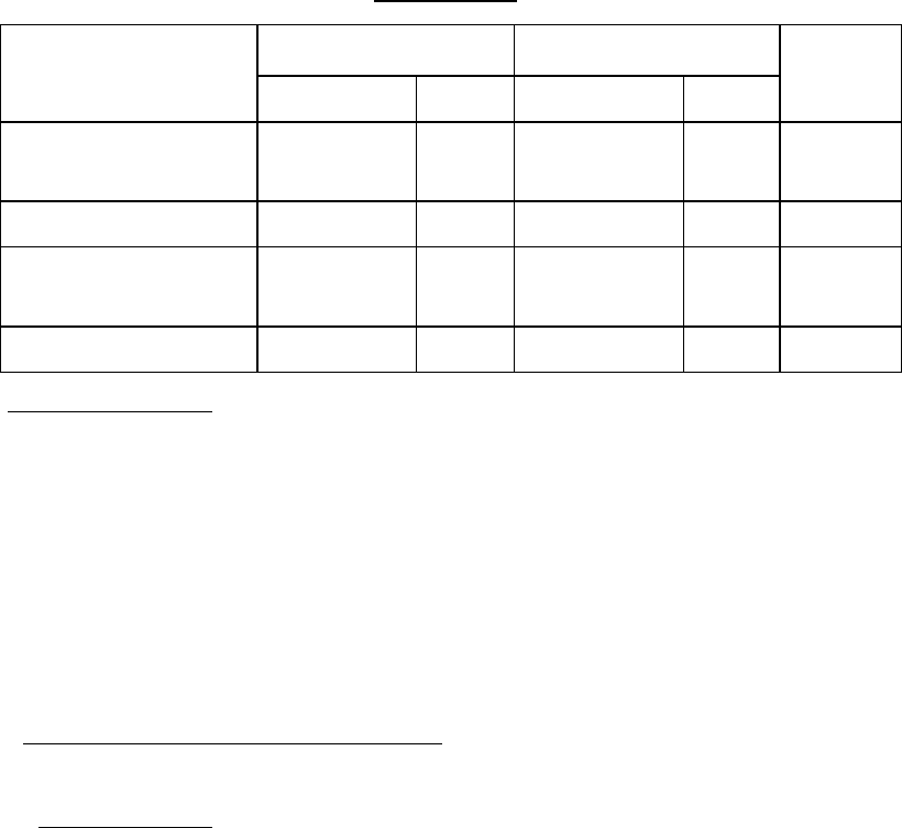
TABLE III. Device screening - Continued.
Screen
Class level S Class level B Reference
paragraph
Method Reqmt. Method Reqmt.
Seal
Fine
Gross
1014 100% 1014 100% 3.4.8
Radiographic 2012 two views 100%
3.4.12
Qualification or quality
conformance inspection
test sample selection
See 3.5
See 3.5
External visual 2009 100% 2009 100% 3.4.13
3.4.2 Internal visual inspection
. Internal visual inspection shall be performed to the requirements of method 2010,
condition A for class level S devices and condition B for class level B devices. Devices awaiting preseal inspection, or other
accepted, unsealed devices awaiting further processing shall be stored in a dry, inert, controlled environment until sealed.
Unless otherwise specified, at the manufacturer's option, test samples for group B, bond strength may be randomly selected
prior to or following internal visual, prior to sealing provided all other specification requirements are satisfied (e.g., bond
strength requirements shall apply to each inspection lot, bond failures shall be counted even if the bond would have failed
internal visual exam).
The alternate procedure of 3.4.2.1 shall be used when any of the following criteria are met:
a. Minimum horizontal geometry is less than three microns.
b. Metallization consists of two or more levels.
c. Opaque materials mask design features.
3.4.2.1 Alternate procedures for class level B microcircuits
. Alternate procedures may be used on an optional basis on
any microcircuit, provided that the conditions and limits of the alternate procedures are submitted to, and approved by the
preparing activity, or the acquiring activity.
3.4.2.1.1 Alternate procedures
. The deletions and the changes stated herein are allowable only if the requirements of
alternate 1 or alternate 2 are met.
Alternate 1: The deletions and the changes stated in 3.4.2.1.1a. are allowable for complex monolithic microcircuits
for class level B product only if the requirements of 3.4.2.1.1.b and 3.4.2.1.1.c are imposed and any
of the following conditions exists.
1. Minimum horizontal geometry is less than 3 micrometers (µm).
2. Interconnects consisting of two or more levels.
3. Opaque materials mask design features.
a. For inspection of each microcircuit die, delete the inspection criteria of 3.1.1, 3.1.2, 3.1.3, 3.1.4, 3.1.5, 3.1.6, 3.1.7,
and 3.2.5 of condition B of method 2010 and for use in conjunction with alternate procedures, add 3.1.1.1, 3.1.1.2,
3.1.1.6, 3.1.3, 3.1.4, and 3.2.5 to the low magnification inspection of method 2010.
b. Temperature cycling (3.4.5). The minimum total number of temperature cycles shall be 50. The manufacturer
may reduce the number of temperature cycles from 50 to the 10 required as part of normal screening based upon
data justifying the reduction in temperature cycles approved by the preparing activity and an approved plan which
shall include the following criteria:
MIL-STD-883F
METHOD 5010.4
18 June 2004
9
(1) Reduction of test must be considered separately for each wafer fabrication line and each die family.
(2) The manufacturer shall demonstrate that the wafer fabrication line that produces product which will involve
reduction of temperature cycles is capable and in process control.
(3) The manufacturer shall perform a high magnification visual inspection on a small sample of devices (e.g.,
5(0)) to monitor the process. This inspection may be performed at wafer level.
c. Special electrical screening tests shall be applied to each microcircuit die at the wafer, individual die (chip) and
packaged, or both, microcircuit level in accordance with the requirements of MIL-STD-883, method 5004, 3.3.2.
The conditions and limits of the electrical tests (in table III format) shall be submitted to the preparing activity for
approval and subsequently maintained on file with the qualifying activity. These special screens are in addition to
the required electrical parametric tests which the device must pass and shall be designed to screen out devices
with defects that were not inspected to the full criteria of 3.4.3 (internal visual). Due to the nature of these tests,
they are not to be repeated as part of the qualification and quality conformance procedures.
Alternate 2: The requirements and conditions for use of this alternate are contained in appendix A of method
5004. This option applies to both class level B and class level S microcircuits.
3.4.3 Stabilization bake
. Stabilization bake is not required for class level S or class level B product unless specified in the
device specification or drawing.
3.4.4 Visual inspection for damage
. The manufacturer may inspect for damage after each screening step. Damaged
devices shall be removed from the lot.
3.4.5 Temperature cycling or thermal shock
. All devices shall be subjected to the requirements of temperature cycling or
thermal shock. The device specifications or drawing shall specify which screen shall be employed. Temperature cycling
shall be in accordance with MIL-STD-883, method 1010, condition C minimum. For class level B, this test may be replaced
with thermal shock in accordance with MIL-STD- 883, method 1011, condition A minimum.
3.4.6 Constant acceleration
. All devices shall be subjected to constant acceleration, in the Y
1
axis only, in accordance
with MIL-STD-883, method 2001, condition E (minimum). Microcircuits which are contained in packages which have an
inner seal or cavity perimeter of two inches or more in total length or have a package mass of five grams or more may be
treated in accordance with provisions below as an alternate to this procedure. Delete test condition E and replace with test
condition D. Unless otherwise specified, the stress level for large, monolithic microcircuit packages shall not be reduced
below condition D. If the stress level specified is below condition D, the manufacture shall have data to justify this reduction
and this data must be maintained and available for review by the preparing or acquiring activity. The minimum stress level
allowed is condition A.
3.4.7 Particle impact noise detection test (PIND)
. Testing to be performed in accordance with appendix A of
MIL-PRF-8535, A.4.6.3. The PIND test may be performed in any sequence after temperature cycling and prior to final
electrical test.
3.4.8 Seal (fine and gross leak) testing
. For class level S devices seal testing may be performed in any sequence
between the final electrical test and external visual, but it shall be performed after all shearing and forming operations on the
terminals. For class level B devices, fine and gross seal test shall be performed separate or together in any sequence and
order between 3.4.7 and 3.4.13 and they shall be performed after all shearing and forming operations on the terminals.
When the 100 percent seal screen cannot be performed following all shearing or forming operations (i.e., flat packs, brazed
lead packages, and chip carriers) the seal screen shall be done 100 percent prior to those shearing and forming operations
and a sample test using sample size number of 45 (C = 0) shall be performed on each inspection lot following these
operations to verify integrity. For devices with leads that are not glass-sealed and that have a lead pitch less than or equal
to 1.27 mm (0.050 inch), the sample seal test shall be performed using an acceptance criteria of a quantity (accept number)
of 15 (0). If sample fails the sample acceptance criteria, all devices in the inspection lot represented by the sample tested
shall be subjected to and pass 100 percent fine and gross leak seal screens.
*

MIL-STD-883F
METHOD 5010.4
18 June 2004
10
3.4.9 Electrical measurements.
3.4.9.1 Interim (pre- and post-burn-in) electrical parameters
. Interim (pre- and post-burn-in) electrical testing shall be
performed when specified, to remove defective devices prior to further testing or to provide a basis for application of percent
defective allowable (PDA) criteria when a PDA is specified. The PDA shall be 5 percent or one device, whichever is greater.
This PDA shall be based, as a minimum, on failures from group A, subgroup 1 plus deltas (in cases where delta parameters
are specified) with the parameters, deltas, and any additional subgroups (or subgroups tested in lieu of A-1) subject to the
PDA as specified in the applicable device specification or drawing. If no device specification or drawing exists, subgroups
tested shall at least meet those of the most similar device specification or Standard Microcircuit Drawing. In addition, for
class level S the PDA shall be 3 percent (or one device, whichever is greater) based on failures from functional parameters
measured at room temperature. For class level S screening, where an additional reverse bias burn-in is required, the PDA
shall be based on the results of both burn-in tests combined. The verified failures after burn-in divided by the total number
of devices submitted in the lot or sublot for burn-in shall be used to determine the percent defective for that lot, or sublot and
the lot or sublot shall be accepted or rejected based on the PDA for the applicable device class. Lots and sublots may be
resubmitted for burn-in one time only and may be resubmitted only when the percent defective does not exceed twice the
specified PDA, or 20 percent, whichever is greater.
3.4.9.2 Pattern failures
. Pattern failure criteria may be used as an option for class level B, provided that:
a. Inspection lot size is less than 500 devices.
b. Pre burn-in electrical testing is done.
3.4.9.2.1 Pattern failures criteria
. A maximum number of pattern failures (failures of the same part type when the failures
are caused by the same basic failure mechanism) shall apply as specified in the acquisition document. If not otherwise
specified, the maximum allowable pattern failures shall be five. Accountability shall include burn-in through final electrical
test.
3.4.9.2.2 Pattern failure resubmission
. When the number of pattern failures exceeds the specified limits, the inspection
lot shall be rejected. At the manufacturer's option, the rejected lot may be resubmitted to burn-in one time provided:
a. The cause of the failure has been evaluated and determined.
b. Appropriate and effective corrective action has been completed to reject all devices affected by the failure cause.
c. Appropriate preventive action has been initiated.
3.4.10 Burn-in
. Device burn-in shall be performed in accordance with the requirements of method 1015 conditions A, B,
C, D, or E. Regardless of power level, devices shall be able to be burned-in at their maximum rated operating temperature.
For devices whose maximum operating temperature is stated in terms of ambient temperature, T
A
, table I of method 1015
applies. For devices whose maximum operating temperature is stated in terms of case temperature, T
C
, and where the
ambient temperature would cause T
J
to exceed 200°C for class level B or 175°C for class level S, the ambient operating
temperature may be reduced during burn-in from 125°C to a value that will demonstrate a T
J
between 175°C and 200°C (for
both class levels S and B) and T
C
equal to or greater than 125°C without changing the test duration. Data supporting this
reduction shall be available to the acquiring and qualifying activities upon request.
3.4.11 Final electrical measurements
. Final electrical testing of microcircuits shall assure that the microcircuits tested
meet the electrical requirements of the applicable device specification or drawing and shall include, as a minimum, the tests
of group A, subgroups 1, 2, 3, 4 or 7, 5 and 6, or 8, and 9.
3.4.12 Radiographic
. The radiographic screen may be performed in any sequence after PIND test and before external
visual inspection. Only one view is required for flat packages and leadless chip carriers having lead (terminal) metal on four
sides.
3.4.13 External visual inspection
. All devices shall be inspected in accordance with MIL-STD-883, method 2009, prior to
acceptance for shipment