MIL- STD-883F 2004 TEST METHOD STANDARD MICROCIRCUITS.pdf - 第676页
MIL-STD-883F METHOD 5010.4 18 June 2004 26 APPENDIX II W AFER LOT ACCEPTANCE 10. SCOPE 10.1 Scope . This appendi x establi shes t he requir ement for wafer lot acceptanc e of mic rocirc uit wafer s int ended for c lass l…

MIL-STD-883F
METHOD 5010.4
18 June 2004
25
APPENDIX I
30.11. Reliability evaluation
.
a. How is the reliability of the process proven? It is done via:
Standard evaluation chips (SECs) or reliability evaluation chips?
Test dice with specialized/optimized test structures?
b. If such vehicles do not exist, how is the processing shown to be free of reliability hazards?
c. How can the power buses be guaranteed to be within current density specifications at all times and under all
conditions?
d. For CMOS technology, how is a latch-up free process assured?
e. For bipolar technology, is any radiation hardness characterization done?
30.12. Documentation
.
a. What are the procedures for certifying and controlling the configuration of software?
b. What are the procedures outlining in detail the process flows for computer-aided
design/manufacture/engineering/test (CAD/M/E/T)?
c. If neither of above is available, when will they be available?

MIL-STD-883F
METHOD 5010.4
18 June 2004
26
APPENDIX II
WAFER LOT ACCEPTANCE
10. SCOPE
10.1 Scope
. This appendix establishes the requirement for wafer lot acceptance of microcircuit wafers intended for class
level B and level S use. The performance of each wafer shall be evaluated individually and independently of the
performance of other wafers in the lot. This wafer lot acceptance procedure is based on fabrication specification adherence
(in accordance with appendix A of MIL-PRF-38535 and the manufacturer's documented fabrication procedures), physical
testing, and electrical testing of suitable process monitors (PM's).
This method can be used only on a fabrication line that has Appendix A of MIL-PRF-38535 certification or control and has
successfully instituted the required checks. Wafers failing any process specification (with the exception of acceptable
rework instances) shall be removed from further processing.
This method is restricted to a well characterized and baselined process. By characterized, it is meant that a fabrication line
has been adequately described in relation to the capabilities of the process. Baselined refers to the existence of a well
defined process parameter target value with associated variances (based on characterization data) against which the actual
wafer to wafer process data is measured to determine acceptability.
A collection of test structures which can provide the parametric data as well as additional yield indicators is referred to as a
"process monitor" (PM). A statistically valid number of PM's shall be provided on each wafer. The PM may be either
stepped onto every wafer in dedicated drop-in die locations, incorporated into kerf locations, or located on each die, such
that they can be probed at the conclusion of processing up to and including final metallization and passivation (glassivation).
Table I presents a minimum listing of structures which make up a PM. The manufacturer shall see PM parametric limits as
called for by design rules and process rules, or both. Probe pads shall be designed to conform to the 2 x N (NIST)
dimensions.
20. APPLICABLE DOCUMENTS. (This section is not applicable to this document.)
30. APPARATUS. Suitable electrical measurement equipment necessary to determine compliance with applicable
acquisition documents and other apparatus as required in the referenced test methods.
40. PROCEDURE. There are three phases to wafer acceptance:
a. Processing to the manufacturer's fabrication baseline and documented fabrication procedures.
b. Visual/SEM inspection.
c. PM evaluation.
Wafers failing any test (with the exception of acceptable rework instances in accordance with appendix A of
MIL-PRF-38535) shall be removed from the lot.
MIL-STD-883F
METHOD 5010.4
18 June 2004
27
APPENDIX II
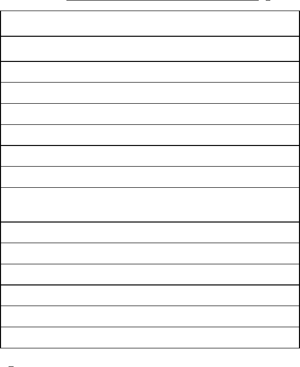
TABLE I. Minimum suggested set of structures used in a PM
. 1/
N-channel transistors for measuring threshold voltages (minimum and
maximum geometries)
P-channel transistors for measuring threshold voltages (minimum and
maximum geometries)
Field threshold device(s)
Leakage current structures
Sheet resistance measurement structures
N-channel gain structures (KN)
P-channel gain structures (Kp)
Oxide breakdown structures (gates, intermetal, and field)
Contact chains (to be sufficient length to allow accurate measurement
of the contact resistance typically found on a device, with diagnostic
procedures to isolate failures)
Metal to poly
Metal 1 to metal 2 via resistance (where applicable)
Metal to diffusion
SEM step coverage checking structures for metal step coverage analysis
Alignment verniers
Functional circuits (e.g., ring oscillator, delay chains, etc.
1/ Appropriate structures for other technologies shall be developed.