MIL- STD-883F 2004 TEST METHOD STANDARD MICROCIRCUITS.pdf - 第677页
MIL-STD-883F METHOD 5010.4 18 June 2004 27 APPENDIX II TABLE I. Mini mum suggest ed set of struc tures us ed in a PM . 1 / N-channel transist ors for measuring threshold voltages (minimum and max imu m geo me tri es) P-c…

MIL-STD-883F
METHOD 5010.4
18 June 2004
26
APPENDIX II
WAFER LOT ACCEPTANCE
10. SCOPE
10.1 Scope
. This appendix establishes the requirement for wafer lot acceptance of microcircuit wafers intended for class
level B and level S use. The performance of each wafer shall be evaluated individually and independently of the
performance of other wafers in the lot. This wafer lot acceptance procedure is based on fabrication specification adherence
(in accordance with appendix A of MIL-PRF-38535 and the manufacturer's documented fabrication procedures), physical
testing, and electrical testing of suitable process monitors (PM's).
This method can be used only on a fabrication line that has Appendix A of MIL-PRF-38535 certification or control and has
successfully instituted the required checks. Wafers failing any process specification (with the exception of acceptable
rework instances) shall be removed from further processing.
This method is restricted to a well characterized and baselined process. By characterized, it is meant that a fabrication line
has been adequately described in relation to the capabilities of the process. Baselined refers to the existence of a well
defined process parameter target value with associated variances (based on characterization data) against which the actual
wafer to wafer process data is measured to determine acceptability.
A collection of test structures which can provide the parametric data as well as additional yield indicators is referred to as a
"process monitor" (PM). A statistically valid number of PM's shall be provided on each wafer. The PM may be either
stepped onto every wafer in dedicated drop-in die locations, incorporated into kerf locations, or located on each die, such
that they can be probed at the conclusion of processing up to and including final metallization and passivation (glassivation).
Table I presents a minimum listing of structures which make up a PM. The manufacturer shall see PM parametric limits as
called for by design rules and process rules, or both. Probe pads shall be designed to conform to the 2 x N (NIST)
dimensions.
20. APPLICABLE DOCUMENTS. (This section is not applicable to this document.)
30. APPARATUS. Suitable electrical measurement equipment necessary to determine compliance with applicable
acquisition documents and other apparatus as required in the referenced test methods.
40. PROCEDURE. There are three phases to wafer acceptance:
a. Processing to the manufacturer's fabrication baseline and documented fabrication procedures.
b. Visual/SEM inspection.
c. PM evaluation.
Wafers failing any test (with the exception of acceptable rework instances in accordance with appendix A of
MIL-PRF-38535) shall be removed from the lot.

MIL-STD-883F
METHOD 5010.4
18 June 2004
27
APPENDIX II
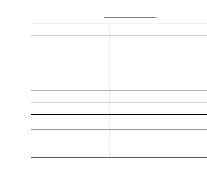
TABLE I. Minimum suggested set of structures used in a PM
. 1/
N-channel transistors for measuring threshold voltages (minimum and
maximum geometries)
P-channel transistors for measuring threshold voltages (minimum and
maximum geometries)
Field threshold device(s)
Leakage current structures
Sheet resistance measurement structures
N-channel gain structures (KN)
P-channel gain structures (Kp)
Oxide breakdown structures (gates, intermetal, and field)
Contact chains (to be sufficient length to allow accurate measurement
of the contact resistance typically found on a device, with diagnostic
procedures to isolate failures)
Metal to poly
Metal 1 to metal 2 via resistance (where applicable)
Metal to diffusion
SEM step coverage checking structures for metal step coverage analysis
Alignment verniers
Functional circuits (e.g., ring oscillator, delay chains, etc.
1/ Appropriate structures for other technologies shall be developed.
MIL-STD-883F
METHOD 5010.4
18 June 2004
28
APPENDIX II
40.1 Processing
. Table II presents a minimum checkpoint list for wafer processing. If certain parameter values are
proprietary, they may be presented in normalized or other specialized form.
TABLE II. In-process check points
.
Process step
Inspection
Incoming material inspection Water, wafers, chemicals, gasses
Photolithography Spin speed, thickness, critical
dimension measurements, alignment,
post development visual inspection
(100X)
Oxidation Index of refraction, flatband, and
threshold voltage shifts, thicknesses
Diffusion Resistivity
Ion implant Resistivity, range, species
Deposition Thickness, resistivity, index of
refraction
Etching Critical dimension measurements,
etch rates, end point detection
SEM Step coverage (all metallization layers)
40.2 Visual/SEM inspection
. Visual inspection of photo resist (PR) patterns, alignment verniers, and critical dimension
measurements shall be made after each PR develop/bake operation. Following every etch and every ion implant, PR mask
stripped wafers shall be inspected for proper PR removal, damage, or other defects, and defective wafers removed from the
lot for scrap or for rework.
In-line nondestructive SEM inspection in accordance with MIL-STD-883, method 2018, shall be performed on each wafer lot.
One wafer from each metallization level shall be randomly selected for inspection. SEM inspection for each level may be
reduced to a weekly basis for each fabrication process when five consecutive lots pass inspection for the given level. If a
metallization level fails the weekly inspection, then lot by lot inspection shall be required until five consecutive lots again
pass. Wafers failing to meet the requirements of the test method shall be removed from processing. Wafer lot acceptance
shall be in accordance with table IV herein.