MIL- STD-883F 2004 TEST METHOD STANDARD MICROCIRCUITS.pdf - 第705页
MIL-STD-883F METHOD 5013 27 July 199 0 1 METHOD 5013 W AFER FABRICATION CONTROL AND W AFER ACCEPTANC E PROCEDURES FOR PROC ESSED GaAs W AFERS 1. PURPOSE . This method spec ifi es wafer fabr icati on contr ol and wafer ac…
MIL-STD-883F
METHOD 5012.1
27 July 1990
10
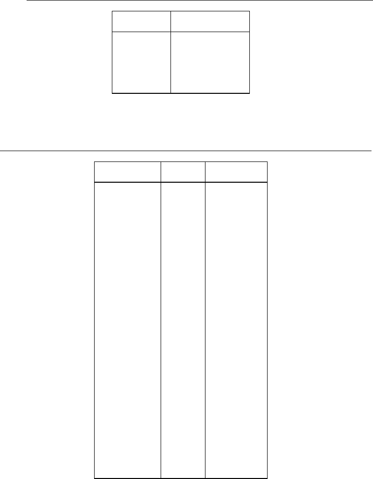
TABLE III. Sample sizes used to obtain lower bound on fault coverage using fault simulation procedure 2.
r
n
0.01
0.015
0.02
0.03
0.04
0.05
6860
3070
1740
790
450
290
NOTE: "n" is the minimum sample size required for a chosen penalty "r".
TABLE IV. Sample sizes used to accept/reject lower bound on fault coverage using fault simulation procedure 3
.
F
n F'
50.0%
55.0%
60.0%
65.0%
70.0%
75.0%
76.0%
77.0%
78.0%
79.0%
80.0%
81.0%
82.0%
83.0%
84.0%
85.0%
86.0%
87.0%
88.0%
89.0%
90.0%
91.0%
92.0%
93.0%
94.0%
95.0%
96.0%
97.0%
98.0%
99.0%
5
6
6
7
9
11
11
12
13
13
14
15
16
17
18
19
20
22
24
26
29
32
36
42
49
59
74
99
149
299
87.1%
89.1%
89.1%
90.6%
92.6%
93.9%
93.9%
94.4%
94.8%
94.8%
95.2%
95.5%
95.8%
96.0%
96.2%
96.4%
96.6%
96.9%
97.2%
97.4%
97.6%
97.9%
98.1%
98.4%
98.6%
98.8%
99.1%
99.3%
99.5%
99.8%
NOTE: For a given minimum required fault coverage "F" simulate "n" faults. If all faults are detected, then conclude that the
actual fault coverage is greater than or equal to "F". Otherwise, conclude that the actual fault coverage is less than "F." The
column labeled "F'" shows the actual fault coverage that has a 50 percent probability of acceptance.

MIL-STD-883F
METHOD 5013
27 July 1990
1
METHOD 5013
WAFER FABRICATION CONTROL AND WAFER ACCEPTANCE
PROCEDURES FOR PROCESSED GaAs WAFERS
1. PURPOSE
. This method specifies wafer fabrication control and wafer acceptance requirements for GaAs monolithic
microcircuits for application in class level B or class level S microcircuits. It shall be used in conjunction with other
documents such as MIL-PRF-38535, MIL-PRF-38534 and an applicable device specification or drawing to establish the
design, material, performance, control, and documentation requirements.
2. APPARATUS
. The apparatus required for this test method includes metallurgical microscopes capable of up to 1,000X
magnification, a scanning electron microscope (SEM), electrical test equipment suitable for the measurement of process
monitor (PM) test structures and other apparatus as required to determine conformance to the requirements of this test
method.
3. PROCEDURE
. The procedures defined herein specify the wafer fabrication controls and wafer acceptance tests
necessary for the production of GaAs wafers compliant to the requirements of this test method.
3.1 Precedence
. Unless otherwise specified in the device specification or drawing, the test requirements and conditions
shall be as given herein.
3.2 Wafer fabrication line controls
.
3.2.1 Process baseline
. The use of this test method is restricted to a well characterized (controlled) and baselined
process. By "characterized" it is meant that the fabrication line has been adequately documented in relation to the
capabilities of the process. "Baselined" refers to the existence of a well defined process parameter target value with
associated variances (based on characterization data) against which the actual wafer to wafer process data is measured to
determine acceptability. The manufacturer shall submit process baseline documentation as specified herein to the acquiring
activity for approval.
3.2.2 Statistical process control
. The manufacturers shall have implemented statistical process control (SPC) for the
wafer fabrication line in accordance with the requirements of EIA-557-A.
3.2.2.1 Alternate visual inspection procedure for class level B microcircuits
. A sample plan for visual inspection in
accordance with 3.1 of test method 2010 may be implemented in lieu of 100 percent visual inspection for processes
controlled by the SPC program. The sample size for inspection shall be identified in the baseline process documentation.
3.2.3 Incoming material evaluation
. Incoming material evaluation shall be performed as documented in the process
baseline to assure compatibility with wafer fabrication specifications and manufacturing procedures.
3.2.4 Electrostatic discharge sensitivity
. The manufacturer shall develop and implement an ESD control program for the
wafer fabrication area.
3.2.5 Failure analysis
. When required by the applicable device specification or drawing, failure analysis shall be
performed on wafers rejected at in-process or acceptance testing.
3.3 Wafer acceptance tests
.
3.3.1 General
. This wafer lot acceptance procedure is based on wafer visual inspection and electrical testing of suitable
process monitors (PMs), see table I. The performance of each wafer shall be evaluated individually. Process monitor
measurements, verifying that the identified baseline parameters are within process limits, will be required from each wafer
lot in accordance with 3.3.2 herein.

MIL-STD-883F
METHOD 5013
27 July 1990
2
3.3.1.1 Process monitor (PM). A process monitor (PM) is a collection of test structures which provide data for the
purposes of process control and determining wafer acceptability. PMs may be either stepped into every wafer in dedicated
drop-in locations, incorporated into kerf locations, located on each die, or combinations of these, such that they can be
probed at the conclusion of processing up to and including final front-side metallization and passivation (glassivation) where
applicable. PM structures, tests and acceptance limits shall be recorded in the baseline document. A suggested list is
shown in table I.
3.3.2 PM evaluation
. Wafer acceptance will be made on a wafer by wafer basis upon the information derived from PM
room temperature testing, which may be performed at any time during the manufacturing cycle. If drop-in PMs are utilized
each wafer shall have a sufficient number of PMs stepped in the center of each of the quadrants to assure the integrity of
the wafer acceptance procedure and the baseline SPC program. For kerf PMs and for PMs on individual die, the probed
PMs shall be located in the center of the wafer and in each of the quadrants. Quadrant PMs shall lie at least one-half of the
distance to the wafer edge away from the wafer center.
3.3.3 Visual/SEM inspection
. Inspection via visual microscopy or SEM shall be performed at critical process steps during
wafer fabrication. When the process flow includes substrate via processing, the backside features shall be visually
inspected to the criteria specified in test method 2010. Inspections may include patterns, alignment verniers, and critical
dimension measurements. Defective wafers shall be removed from the lot for scrap or for rework. Inspection operations,
sampling plans and acceptance criteria shall be documented in the process baseline.
3.3.4 Test results
. When required by the device specification or drawing or for qualification, the following test results shall
be made available for each wafer lot submitted.
a. Results of each test conducted; initial and any resubmissions.
b. Number of wafers accepted/rejected per lot.
c. Number of reworked wafers and reason for rework.
d. Measurements and records of the data for all specified PM electrical parameters.
3.3.5 Defective wafers
. All wafers that fail any test criteria shall be removed at the time of observation or immediately at
the conclusion of the test in which the failure was observed. Rejected wafers may be subjected to approved rework
operations as detailed in the baseline document. Once rejected and verified as an unreworkable failure, no wafer may be
retested for acceptance. Rejected wafers processed in accordance with approved rework procedures shall be resubmitted
to all applicable inspections at the point of rejection and must be found acceptable prior to continuing processing.
3.3.6 Element evaluation
. When specified, upon completion of wafer acceptance based on the baseline SPC program
and PM measurement results, 100 percent static/RF testing at 25°C shall be performed on each individual die. Failures
shall be identified and removed from the lot when the die are separated from the wafer.