MIL- STD-883F 2004 TEST METHOD STANDARD MICROCIRCUITS.pdf - 第73页
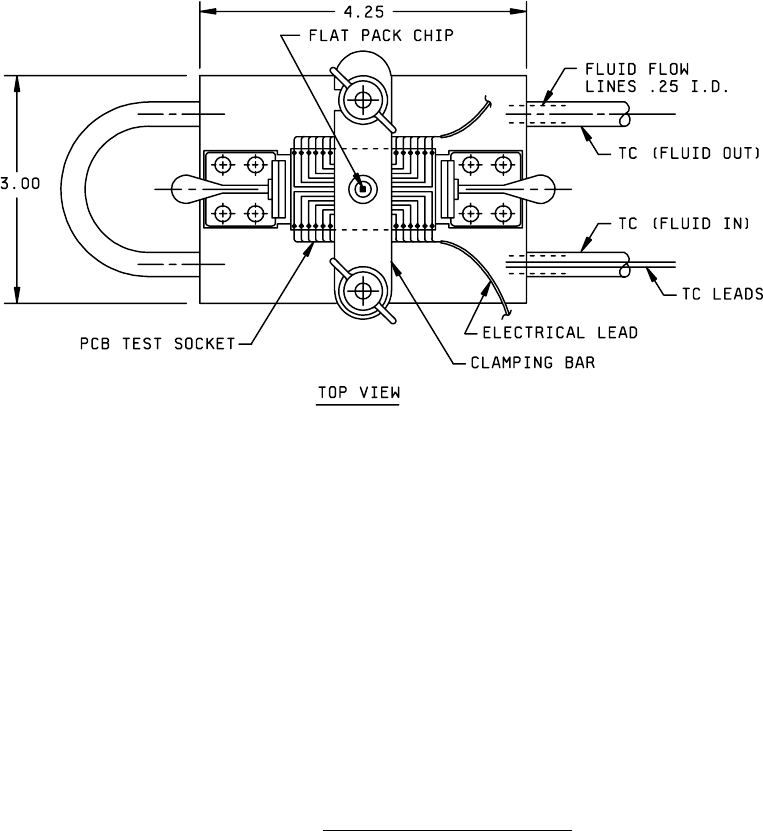
MIL-STD-883F METHOD 1012.1 4 November 1980 9 FIGURE 1012-1. Temperatur e contr olled heat s ink .

MIL-STD-883F
METHOD 1012.1
4 November 1980
8
3.4 Calculations of R
θJR
and t
JR
.
3.4.1 Calculations of package thermal resistance
. The thermal resistance of a microelectronic device can be calculated
when the peak junction, average junction, or region junction temperature, T
J(Peak)
, T
J(Avg)
, or T
J(Region)
, respectively, has been
measured in accordance with procedures outlined in sections 3.1 and 3.2. If the total package capability is to be assessed,
then rated power P
D(Packages)
should be applied to the device under test. For quality control purposes the power dissipation in
the single test junction P
H(Element)
can be used in the calculation of thermal resistance.
With the data recorded from each test, the thermal resistance shall be determined from:
R
θJC(PEAK)
= T
J(PEAK)
- T
C
, junction peak-to-case;
P
D(Package)
R
θJC(Avg)
= T
J(Avg)
- T
C
, junction average-to-case; or
P
D(Package)
R
θJC(Region)
= T
J(Region)
- T
C
, junction region-to-case;
P
D(Package)
For calculations of the junction element thermal resistance, P
D(Element)
should be used in the previous equations. Note that
these thermal resistance values are independent of the heat sinking technique for the package. This is possible because
the case or chip carrier (reference) temperature is measured on the package itself in an accessible location which provides
a representative temperature in the major path of heat flow from the chip to the heat sink via the package.
3.4.2 Calculation of package thermal response time
. The thermal response time of a microelectronic device can be
calculated when the peak junction, average junction, or region junction temperature, T
J(Peak)
, T
J(Avg)
, or T
J(Region)
, respectively,
has been measured as a function of time in accordance with procedures outlined in section 3.3. If the total package
capability is to be assessed, then rated power P
D(Package)
should be applied to the device under test. For quality control
purposes the power dissipation in the single test junction P
D(Element)
can be used in the calculation of thermal response time.
With the data recorded from each test, the thermal response time shall be determined from a curve of junction temperature
versus time from the time of application or removal of the heating power to the time when the junction temperature reaches a
stable value. The thermal response time is 0.9 of this difference.
4. SUMMARY
. The following details shall be specified in the applicable acquisition document:
a. Description of package; including number of chips, location of case or chip carrier temperature measurement(s),
and heat sinking arrangement.
b. Test condition(s), as applicable (see section 3).
c. Test voltage(s), current(s) and power dissipation of each chip.
d. Recorded data for each test condition, as applicable.
e. Symbol(s) with subscript designation(s) of the thermal characteristics determined to verify specified values of
these characteristics, as applicable.
f. Accept or reject criteria.
MIL-STD-883F
METHOD 1012.1
4 November 1980
9
FIGURE 1012-1. Temperature controlled heat sink
.
MIL-STD-883F
METHOD 1012.1
4 November 1980
10
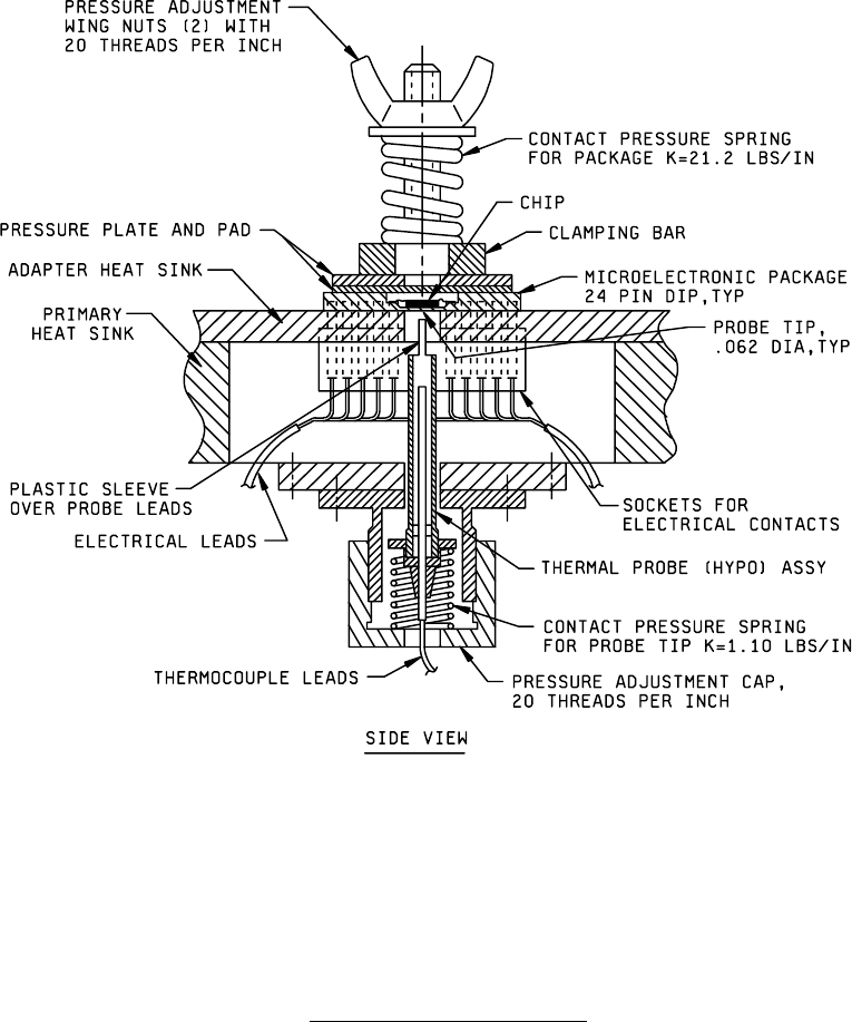
FIGURE 1012-1. Temperature controlled heat sink
- Continued.