17-2756-ASM Broschüre ASM AP EN_171020 - 第10页
Die Attach & SMT Deposition 1 2 Printing Stencil technology T ruly unique: SIPLACE CA combines bare-chip and SMT placement Do you combine bare-die placement with the placement of classic SMT components in your produc…
TRS Tooling
TRS tooling
Flux printing
Die Attach & SMT Encapsulation Singulation
WLP Inspection,
Text & Packing
3
4
5
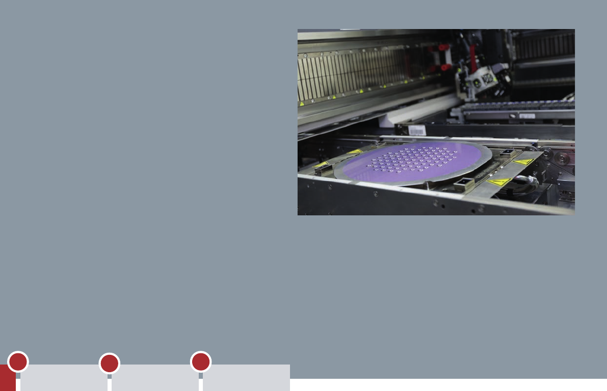
Flux and solder paste
With the rst two printing processes,
ux or solder paste are applied to the
substrates via classic stencil printing
with multi-level DEK e-form stencils.
The versatile DEK printer software ma-
kes it easy to adjust all relevant opera-
ting parameters.
Ball drop
For the ball drop process, i.e. the appli-
cation of solder balls onto the underside
of the SiPs, the DEK Galaxy provides
another solution. With its DirEKt Ball
Placement Option, solder balls can be
applied individually (ball attachment).
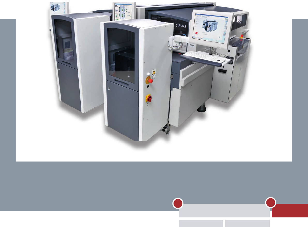
DEK Galaxy
Reliable printing in chip assembly
▪ For demanding wafer, substrate and circuit board
applications
▪ Process Alignment Capability: 2 Cpk @ ±12.5 µm 6 sigma
▪ ProFlow
®
DirEKt Imaging technologies for high-precision
ball placements
▪ Modular: Flexibly configurable with toolings and transport
systems for the widest range of advanced packaging
applications
▪ SMEMA- and HERMES-compatible interfaces to wafer
and flux solutions
▪ Fast: Core cycle time of only 7 seconds
▪ Flexible: Product changeovers take less than 2 minutes
▪ Easy to use: DEK Instinctiv™ software
9
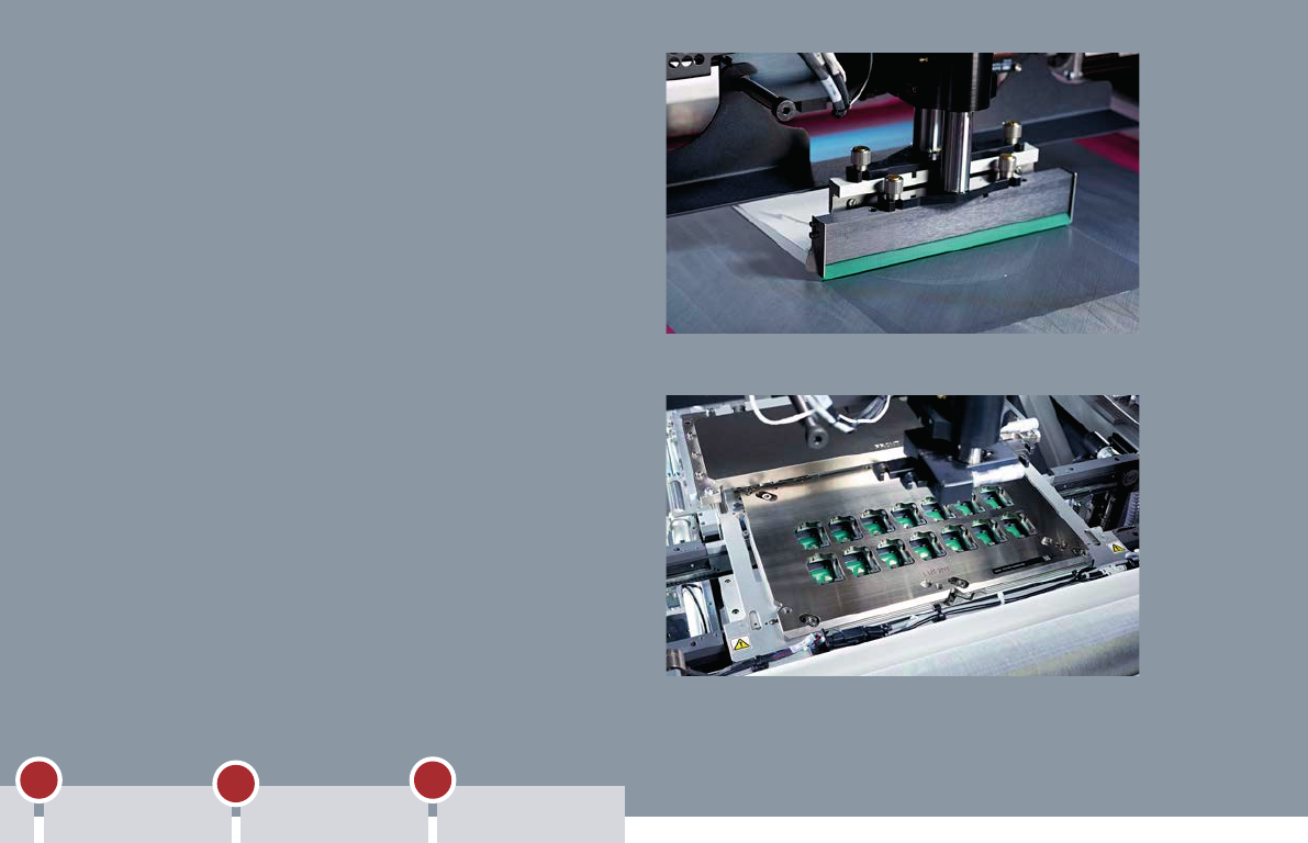
Die Attach & SMTDeposition
1
2
PrintingStencil technology
Truly unique:
SIPLACE CA combines bare-chip and SMT placement
Do you combine bare-die placement with
the placement of classic SMT components
in your production? Or in other words: are
you looking for a universal machine that
you can use to populate large carriers in
panel level packaging as well as for clas-
sic SMT placement applications? These
processes used to be strictly separate –
until now.
Today, ASM is the rst equipment maker
that can offer you more: the SIPLACE CA.
This uniquely innovative solution tears
down the borders between semiconduc-
tor backend and SMT handling. For the
rst time you can run both processes on
a single machine – even simultaneously.
This improves your ef ciency, makes your
processes more stable by reducing the
number of required process steps, and
gives you a leg up on the competition.
High Precision Chip Placement
10
Populated 300 mm (12-inch) carrier for the wafer level fan out process
Die Attach & SMT
Encapsulation Singulation
WLP Inspection,
Text & Packing
3
4
5
Flexible wafer modules enable you to feed
the SIPLACE CA in Die Attach and Flip
Chip process directly from the wafer and
transfer them to panels with exceptional
speed and precision. And thanks to its e-
xible conveyor, you can process substrate-
swith sizes of up to 650 mm × 700 mm.
These features are not the only strengths
of the SIPLACE CA. It also handles the
whole spectrum of classic SMT compon-
ents via tapes and feeders and does it all
with breathtaking speed. With its four SIP-
LACE SpeedStar heads, the SIPLACE CA
processes up to 100,000 SMT component,
42,000 ip-chips or 28,000 die-attach
components per hour.
ASM offers with the SIPLACE CA a global-
ly unique solution that opens up an entrely
new set of possibilities in embedding,
WLFO packaging, and SiP processes.
In addition, the four-gantry SIPLACE CA
provides capacities wherever you need
them. Depending on your current require-
ments, it can apply its capabilities exclusi-
vely to the recon guration of bare dies or
ip chips or the placement of SMT compo-
nents, or a combination of the two.
SIPLACE CA
Closing the gap between chip assembly
and SMT processes
▪ Processes large panels (650 mm × 700 mm) at
maximum speed
▪ Handles SMT components and dies from wafer in a
single machine – perfect for SiP (system-in-package)
production
▪ Maximum placement accuracy
Panels up to 330 mm × 330 mm: 10 µm @ 3 sigma
large panels: 15 µm @ 3 sigma
▪ CPH ratings: up to 100,000 for SMT; up to 42,000 for
flip-chips from wafers; up to 100,000 for die-attach
from wafers
▪ Consistently high placement performance for SMT
components ranging from 0201 to 27 mm × 27 mm
11