17-2756-ASM Broschüre ASM AP EN_171020 - 第12页
Die Attach & SMT Deposition 1 2 Printing Stencil technology Whether fan-in, fan-out or embedded chips – encapsulating and protecting elec- tronic components in epoxy mold com- pounds is an important step in WLP/PLP a…
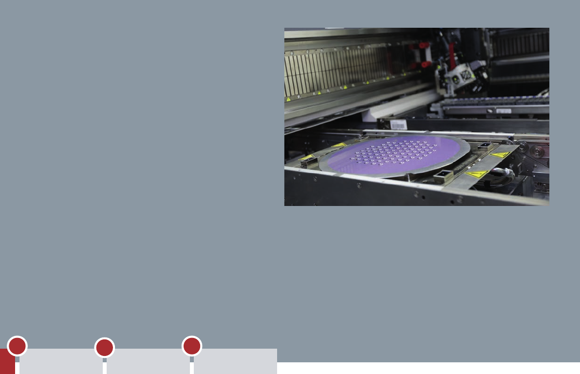
Populated 300 mm (12-inch) carrier for the wafer level fan out process
Die Attach & SMT
Encapsulation Singulation
WLP Inspection,
Text & Packing
3
4
5
Flexible wafer modules enable you to feed
the SIPLACE CA in Die Attach and Flip
Chip process directly from the wafer and
transfer them to panels with exceptional
speed and precision. And thanks to its e-
xible conveyor, you can process substrate-
swith sizes of up to 650 mm × 700 mm.
These features are not the only strengths
of the SIPLACE CA. It also handles the
whole spectrum of classic SMT compon-
ents via tapes and feeders and does it all
with breathtaking speed. With its four SIP-
LACE SpeedStar heads, the SIPLACE CA
processes up to 100,000 SMT component,
42,000 ip-chips or 28,000 die-attach
components per hour.
ASM offers with the SIPLACE CA a global-
ly unique solution that opens up an entrely
new set of possibilities in embedding,
WLFO packaging, and SiP processes.
In addition, the four-gantry SIPLACE CA
provides capacities wherever you need
them. Depending on your current require-
ments, it can apply its capabilities exclusi-
vely to the recon guration of bare dies or
ip chips or the placement of SMT compo-
nents, or a combination of the two.
SIPLACE CA
Closing the gap between chip assembly
and SMT processes
▪ Processes large panels (650 mm × 700 mm) at
maximum speed
▪ Handles SMT components and dies from wafer in a
single machine – perfect for SiP (system-in-package)
production
▪ Maximum placement accuracy
Panels up to 330 mm × 330 mm: 10 µm @ 3 sigma
large panels: 15 µm @ 3 sigma
▪ CPH ratings: up to 100,000 for SMT; up to 42,000 for
flip-chips from wafers; up to 100,000 for die-attach
from wafers
▪ Consistently high placement performance for SMT
components ranging from 0201 to 27 mm × 27 mm
11
Die Attach & SMTDeposition
1
2
PrintingStencil technology
Whether fan-in, fan-out or embedded
chips – encapsulating and protecting elec-
tronic components in epoxy mold com-
pounds is an important step in WLP/PLP
and SiP processes.
Granulate or liquid epoxy resin, different
EMC patterns, wafers or panels as carri-
ers, the degree of automation – there are
many process details that determine the
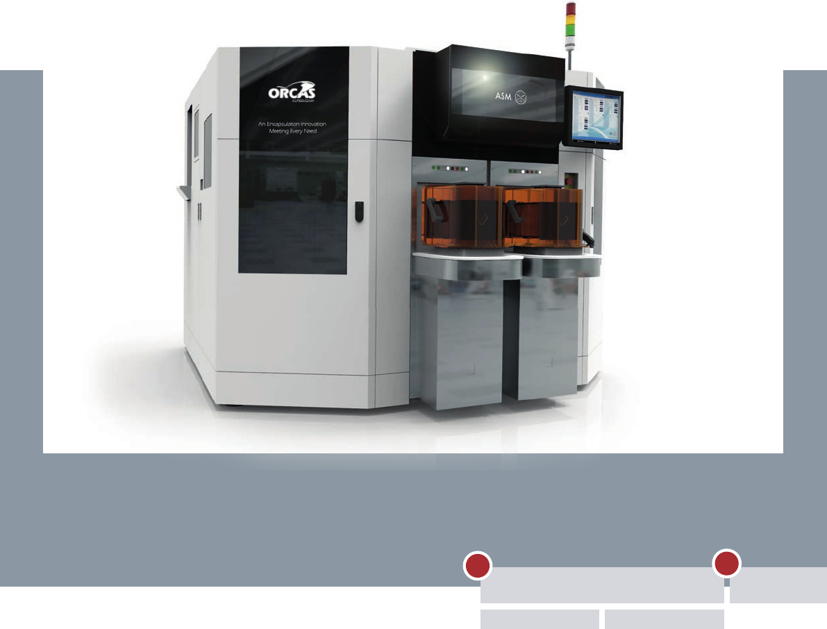
requirements for your solution. ORCAS
(Over-molding of Resin Epoxy Compres-
sion Auto-Panel Encapsulation System) is
the most exible option on the market.
Coplanarity Control
Take closed-loop coplanarity control, for
example. Sensors detect thickness
variations in the substrate and adjust the
tooling accordingly. The SCARA wafer
handling robot can handle wafers that are
warped by up to 3 mm. Thanks to copla-
narity control, ORCAS recognizes and
compensates for even the nest variations
in substrate thickness.
ORCAS also features maximum auto-
mation exibility. With manual load, it is
the perfect solution for small-lot and proto-
type manufacturing, while fully automated
substrate handling and other functions
make it a highly ef cient solution for high-
volume production.
Molding
The efficient encapsulation solution for
advanced packaging: ORCAS
12
Die Attach & SMT
Encapsulation Singulation
WLP Inspection,
Text & Packing
3
4
5
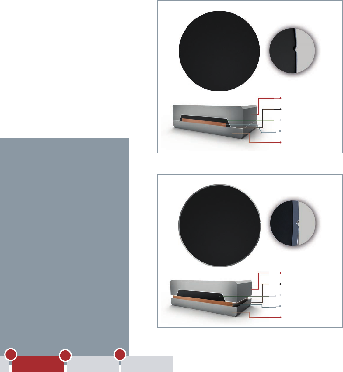
Molding with keep-out zone (KOZ) makes
ORCAS the ideal solution for subsequent
singulation using laser separation. Thanks
to special tooling, the dicing patterns in the
keep-out zone at the edge of the carrier
remain visible after the molding process.
The laser-dicing process takes place with
exceptional precision and thus, without
any other preparatory steps – a prime
example of how ef ciently process chains
in advanced packaging can be integrated
and improved. The result: Improved yield
rates and the ability to make packaging
even more ef cient.
ORCAS
Quick and efficient molding
▪ Panel sizes up to 340 mm × 340 mm
and 12-inch wafers
▪ Closed-loop press system ensures
excellent coplanarity in large-area
molding applications (TTV: 20 µm)
▪ A highly flexible dispensing system
ensures best compound coverage
by processing liquid and granular
encapsulant
▪ Scalable from small-lot and prototype
manufacturing to high-volume
production
▪ One system for die-up and die-down
molding
▪ Two molding options: Molding,
configurable for with keep-out zone
(KOZ) or overmolding
In KOZ molding the edge of the wafer is not covered with EMC to make
the subsequent singulation process more efficient.
Simply clever:
Molding with keep-out zone
Top Mold Case
Film
Molding Compound
Substrate
Bottom Mold Case
Top Mold Case
Film
Molding Compound
Substrate
Bottom Mold Case
In overmolding the whole wafer is covered with molding
compound to also protect the edges.
13