17-2756-ASM Broschüre ASM AP EN_171020 - 第15页
Die Attach & SMT Encapsulation Singulation WLP Inspection, T ext & Packing 3 4 5 15

Die Attach & SMTDeposition
1
2
PrintingStencil technology
Declining component sizes and wafer
thickness, and the desire for more efcien-
cy, i.e. more density on WLP/PLP carriers,
require increasingly accurate and gentle
component singulation capabilities.
Classic saws encounter limitations in
terms of cutting width and accuracy when
they cut into the carrier (for example, with
low-K materials and the resulting threat of
contamination) as well at the end of the
packaging process. In addition, the
packages are subject to mechanical
stresses during the sawing process.
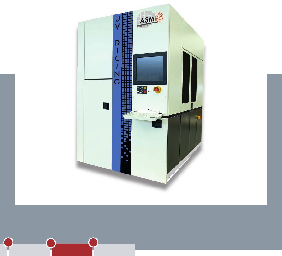
ASM‘s LASER 1205 multi-beam laser
system is the answer to the rising require-
ments in singulation.
At substrate thicknesses of 100 µm, the
cutting width stays below 12-14 µm with a
positioning tolerance of less than < 1 µm.
The machine can cut a wide range of
materials like silicon wafer (Si, SiC etc.)
with thicknesses of up to 250 μm and
EMCs with thicknesses of up to 700 µm.
Thanks to multi-beam technology, signi-
cantly fewer cutting cycles are needed to
separate the wafers. As a result, the ASM
LASER 1205 achieves exceptionally short
cycle times and a correspondingly high
level of productivity.
Singulation
More precision and efficiency:
Singulation with the LASER 1205 multi-beam laser system
LASER 1205
Precise and efficient for silicon and EMC
▪ Enabling technology for fan-in applications
▪ Precise dicing of molding compound and silicon
▪ Higher yield due to minimized dicing street (12-14 µm)
▪ No wafer-chipping since the laser cut is aligned precisely
within the pre-cut position
▪ Seamless transition from fan-in to fan-out with the same basic
packaging platform intact
14
Die Attach & SMT
Encapsulation Singulation
WLP Inspection,
Text & Packing
3
4
5
15
Stencil PrintingDeposition
1
2
PrintingStencil technology
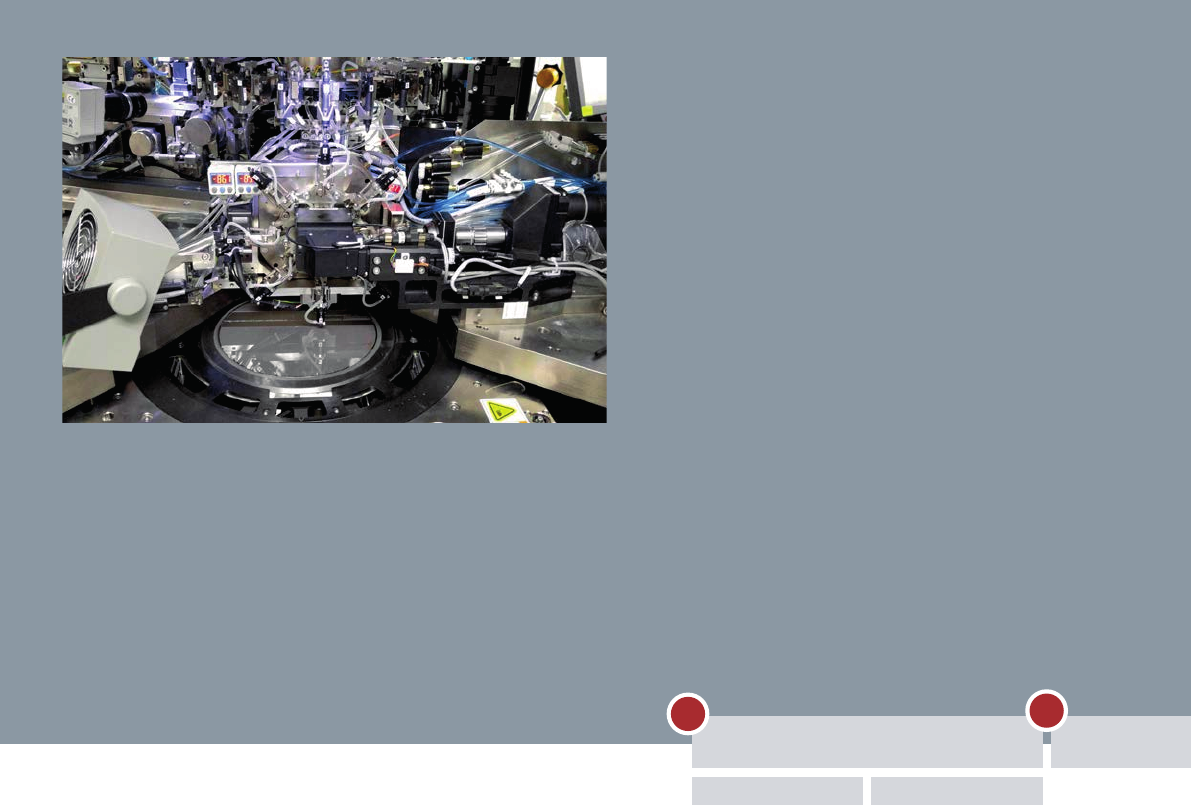
SUNBIRD
Extremely efficient inspection, sorting
and taping
▪ Combines various optical and electrical inspection
and (optional) laser marking capabilities in one
machine
▪ More reliable detection of faults by individual optical
inspection
▪ Maximum speed of 30,000 UPH thanks to turret
system
▪ Contactless alignment and smart chip handling
ensure optimal package protection
▪ Handling of smallest components (0603/0402 metric)
Dies are picked directly from the wafer to the turret system and transported
through various optical inspection and electrical test positions.
Six-side inspection, electrical tests,
laser marking, sorting and taping – the
SUNBIRD system combines a series of
functions in a single machine. And best of
all, thanks to the SUNBIRD turret system,
it does it all with a high degree of speed
and efciency.
In a rst step, the machine picks up the
packages with its ip arm, inspects their
bottom side and passes them to the turret,
where they are inspected from six angles,
tested, and optionally laser-marked.
Thanks to the SUNBIRD‘s smart iPrecise
and iAlign technologies, the alignment of
all components is ensured and optimized
via powerful optics and without any additi-
onal transfers.
Next, the SiP components are gently positi-
oned in tape pockets with automatic Z-axis
alignment, under the continuous check
of a vision system, which was especially
developed for this purpose. That way, even
extremely small, thin and sensitive dies can
be inspected and taped perfectly.
The nal sorting step: Divided by software
into separate classes, the machine places
the components into the tape or different
containers. With processing speeds of up
to 30,000 UPH, SUNBIRD represents a
signicant speed and quality improvement
over traditional systems.
WLP Inspection, Test & Packing
Finalizing your WLP/PLP processes:
SUNBIRD for inspecting, sorting and taping
16