17-2756-ASM Broschüre ASM AP EN_171020 - 第4页
1 2 The process chain for SiP applications combines classic semiconductor and SMT processes. Deposition The rst process step is the deposition of ux and solder paste on the substrate. Thanks to ASM‘s innovative print…
The rising spread of mobile devices and
the Internet of Things (IoT) push the need
for ever smaller modules and components.
Electronics must be increasingly inte-
grated and produced in accordance with
the highest quality standards, but at ever
lower cost.
One response to these challenges is
advanced packaging, which integrates
bare dies or flip-chips with SMT com-
ponents to form ultra-compact systems
(system-in-package, or SiP). Advanced
packaging techniques make it possible to
create complete function modules that can
then be placed efficiently and reliably on
an SMT line.
Separately in the past, now combined.
In the past, the semiconductor – espe-
cially in back-end packaging operations
– and SMT production industries operated
separately from each other. In advanced
packaging, their processes overlap for
the first time. The result: Besides OSATs,
classic electronics manufacturers can
help out the semiconductor industry by
supplementing its operations to meet the
exploding demand for ultra-compact, SMT-
capable function modules. This opens up
an attractive growth market for the electro-
nics production industry.
Only at ASM: Everything from a single
source
ASM is your experienced partner for ente-
ring the advanced packaging market. ASM
is the world’s only equipment supplier with
solutions for all phases and process steps
in the electronics industry – from lead
frame to backend to SMT.
ASM‘s unique process and industry exper-
tise flow into its advanced packaging offe-
rings. This enables ASM to offer solutions
for each specific process from a single
source with complete, integrated solution
chains ranging from sophisticated printing
processes to the combined placement of
dies, flip-chips and SMT components to
molding, singulation, testing and packa-
ging.
ASM is an experienced and innovative
partner that backs you with competent
advice, equipment, and a wide range of
support services. With ASM, the outlook
for your entry into the attractive advanced
packaging market couldn‘t be better.
Advanced Packaging/WLSiP
3
1 2
The process chain for SiP applications
combines classic semiconductor and SMT
processes.
Deposition
The rst process step is the deposition
of ux and solder paste on the substrate.
Thanks to ASM‘s innovative printing tech-
nologies, this can be done quickly and
ef ciently with the precision required for
wafer-level operations.
Multilevel e-formed stencils have become
the standard for this process. With the
additive e-forming process, stencils can be
produced with the ultra- ne apertures and
gradations required for ux/solder paste
printing and wafer bumping.
The ideal platform for this stencil tech-
nology is the powerful and versatile DEK
Galaxy, whose exceptional precision and
exible options make it the ideal solution
for a wide range of printing applications in
the advanced packaging eld.
Placement
SiP require extremely precise machines
that can take components directly from the
wafer as well as from classic tape feeders
and place them onto the various substrates
such as circuit boards, wafers or panels.
In the case of WLSiP, Dies and SMT com-
ponents are placed directly on the wafer.
This is made possible by powerful wafer
handlers for various formats and pickup
processes for bare dies and ip-chips. After
the substrates have been populated, they
go through a re ow process.
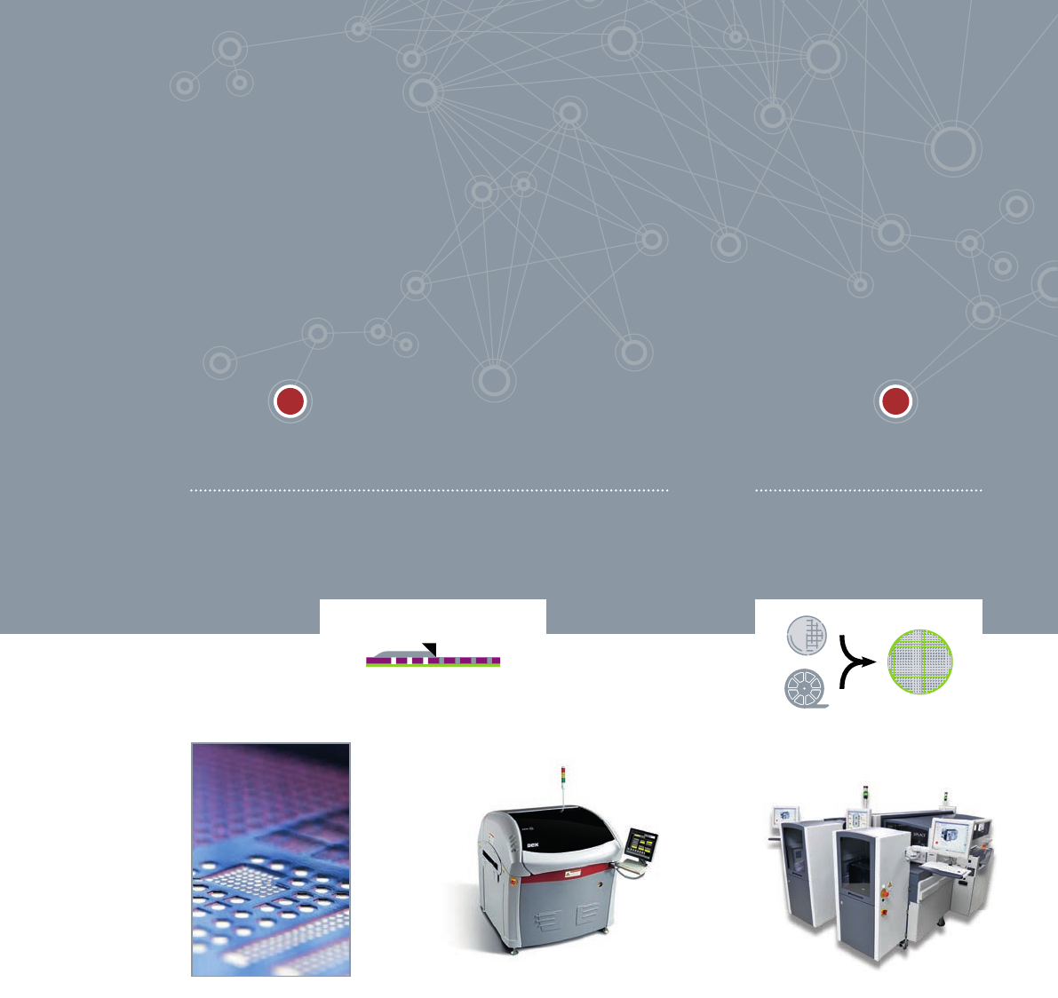
The whole solution chain from a single source
Wafer-level System-in-Package (SiP) Process
DIE ATTACH & SMT
SIPLACE CA
Combined placement from
wafers and SMT feeders
DEPOSITION
EFORM STENCIL
TECHNOLOGY
Ultra-precise multi-level stencils
DEK Galaxy
The solution for printing
and bumping
4
3 4 5
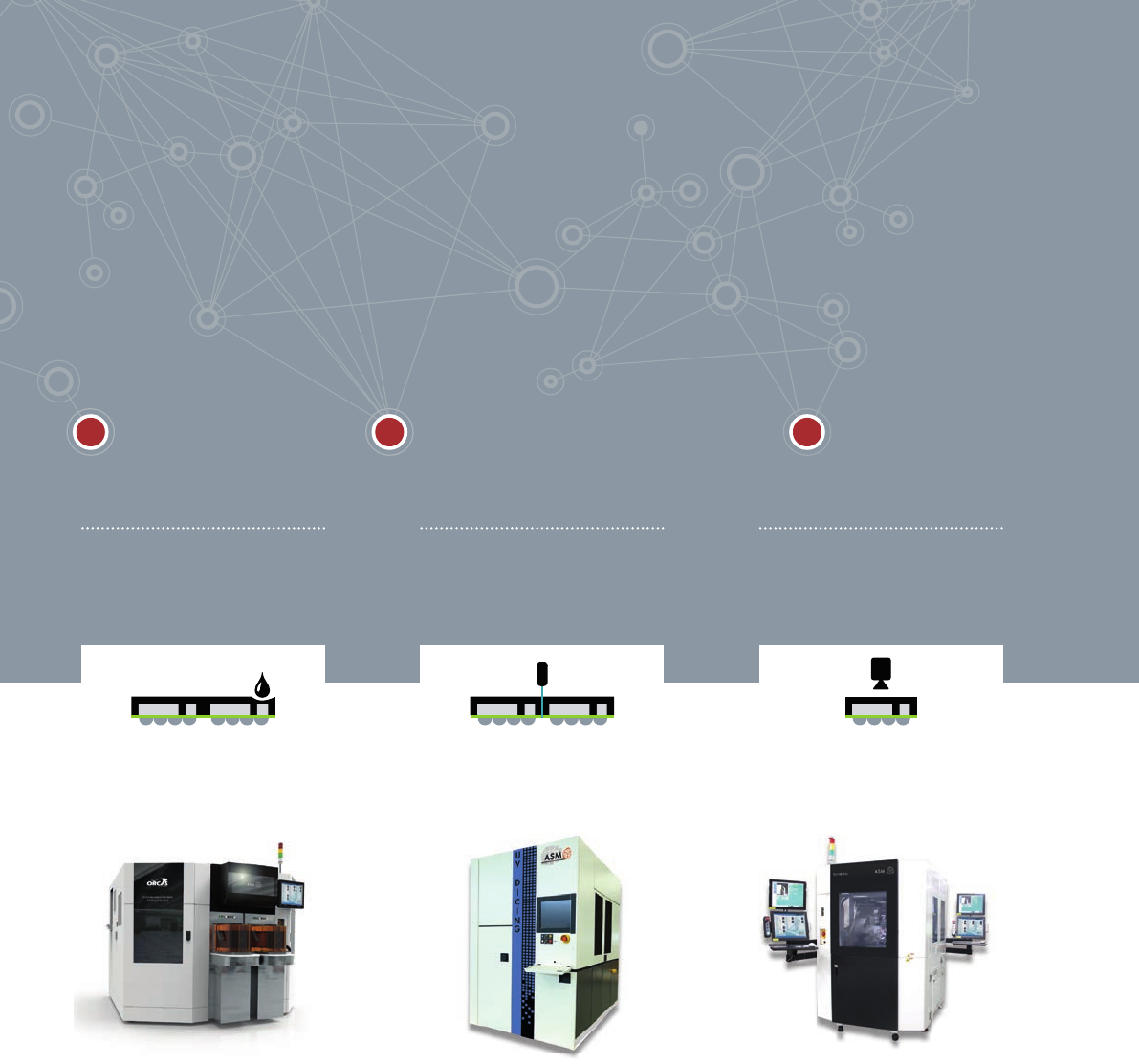
The whole solution chain from a single source
Wafer-level System-in-Package (SiP) Process
ENCAPSULATION
ORCAS
Flexible molding
SINGULATION
LASER 1205
Precise and efficient
laser-cutting
WLP INSPECTION,
TEST & PACKAGING
SUNBIRD
Highly efficient all-in-one
solution
Molding
Next, the substrates with the SiPs is mol-
ded, usually via press-forming with epoxy.
For these and the subsequent SiP process
steps such as redistribution layer in thin-
layer technology, proven tools from the
semiconductor industry is normally used,
which explains why most SiP processes
operate with wafer-shaped panels.
Singulation
In the singulation process, classic saws
have been replaced by laser-based solu-
tions, because they are faster and more
accurate. Even more modern solutions
already operate with multi-beam lasers.
From testing to taping
The SiP must be picked up, optically in-
spected, tested, sorted, marked, labeled,
and packaged in tapes for the placement
process. Modern solutions have turrets and
combine these steps in a single machine.
End-to-end solution chain
All of these steps form a multi-layered,
complex process that can only be managed
with a consistently coordinated solution
chain as well as with lots of experience and
competence. Only ASM can offer this solu-
tion chain from a single source. Check out
the following pages for more details.
5