17-2756-ASM Broschüre ASM AP EN_171020 - 第5页
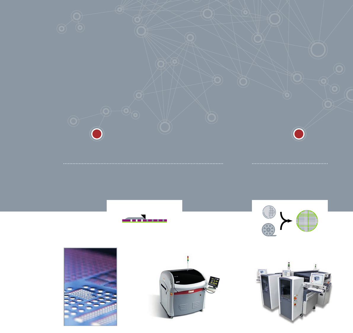
3 4 5 The whole solution chain from a single source W afer-level System-in-Package (SiP) Process ENCAPSULA TION ORCAS Flexible molding SINGULA TION LASER 1205 Precise and efficient laser-cutting WLP INSPECTION, TEST &…
1 2
The process chain for SiP applications
combines classic semiconductor and SMT
processes.
Deposition
The rst process step is the deposition
of ux and solder paste on the substrate.
Thanks to ASM‘s innovative printing tech-
nologies, this can be done quickly and
ef ciently with the precision required for
wafer-level operations.
Multilevel e-formed stencils have become
the standard for this process. With the
additive e-forming process, stencils can be
produced with the ultra- ne apertures and
gradations required for ux/solder paste
printing and wafer bumping.
The ideal platform for this stencil tech-
nology is the powerful and versatile DEK
Galaxy, whose exceptional precision and
exible options make it the ideal solution
for a wide range of printing applications in
the advanced packaging eld.
Placement
SiP require extremely precise machines
that can take components directly from the
wafer as well as from classic tape feeders
and place them onto the various substrates
such as circuit boards, wafers or panels.
In the case of WLSiP, Dies and SMT com-
ponents are placed directly on the wafer.
This is made possible by powerful wafer
handlers for various formats and pickup
processes for bare dies and ip-chips. After
the substrates have been populated, they
go through a re ow process.
The whole solution chain from a single source
Wafer-level System-in-Package (SiP) Process
DIE ATTACH & SMT
SIPLACE CA
Combined placement from
wafers and SMT feeders
DEPOSITION
EFORM STENCIL
TECHNOLOGY
Ultra-precise multi-level stencils
DEK Galaxy
The solution for printing
and bumping
4
3 4 5
The whole solution chain from a single source
Wafer-level System-in-Package (SiP) Process
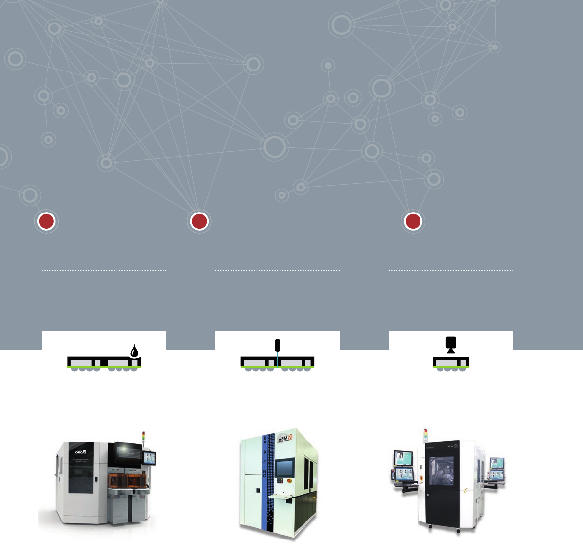
ENCAPSULATION
ORCAS
Flexible molding
SINGULATION
LASER 1205
Precise and efficient
laser-cutting
WLP INSPECTION,
TEST & PACKAGING
SUNBIRD
Highly efficient all-in-one
solution
Molding
Next, the substrates with the SiPs is mol-
ded, usually via press-forming with epoxy.
For these and the subsequent SiP process
steps such as redistribution layer in thin-
layer technology, proven tools from the
semiconductor industry is normally used,
which explains why most SiP processes
operate with wafer-shaped panels.
Singulation
In the singulation process, classic saws
have been replaced by laser-based solu-
tions, because they are faster and more
accurate. Even more modern solutions
already operate with multi-beam lasers.
From testing to taping
The SiP must be picked up, optically in-
spected, tested, sorted, marked, labeled,
and packaged in tapes for the placement
process. Modern solutions have turrets and
combine these steps in a single machine.
End-to-end solution chain
All of these steps form a multi-layered,
complex process that can only be managed
with a consistently coordinated solution
chain as well as with lots of experience and
competence. Only ASM can offer this solu-
tion chain from a single source. Check out
the following pages for more details.
5
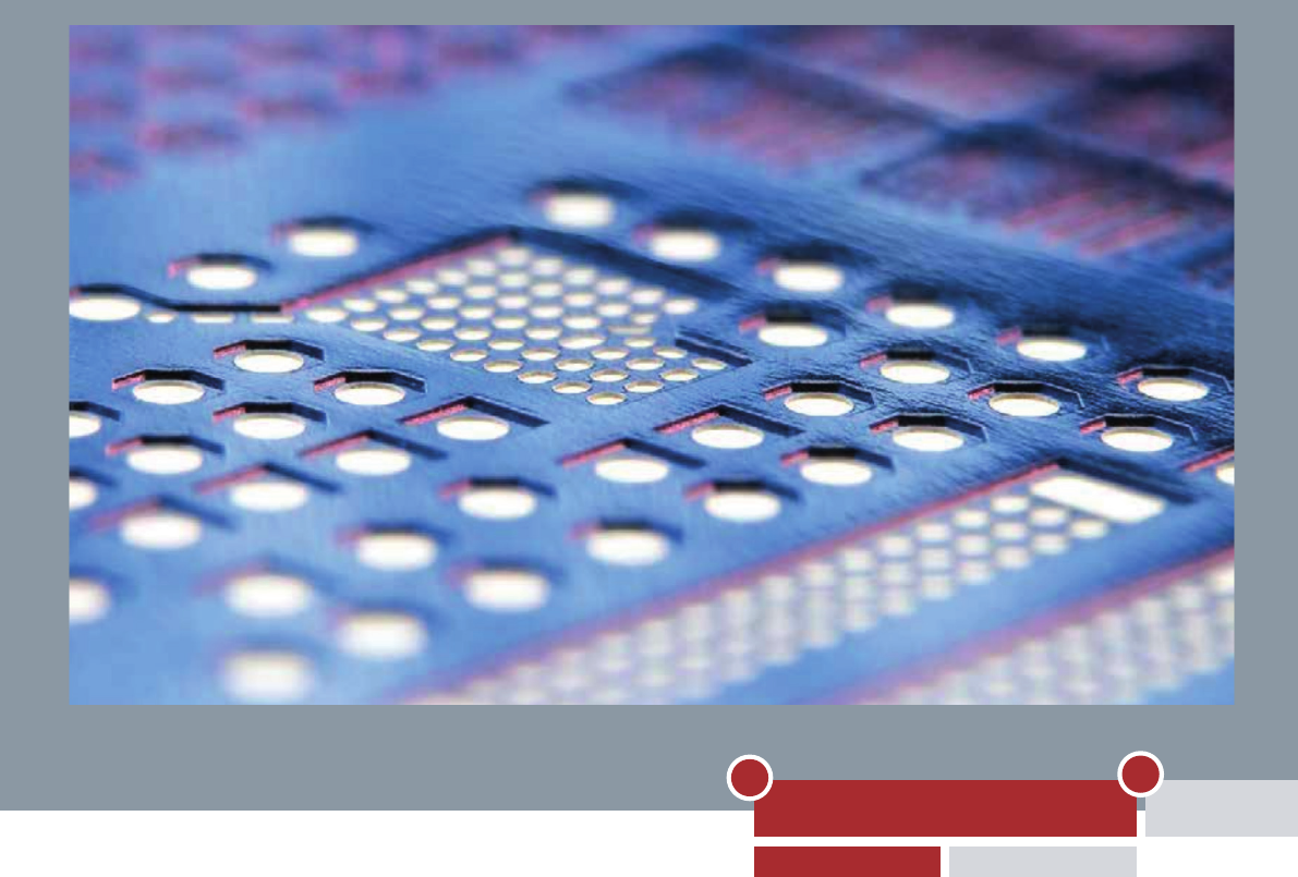
Deposition
PrintingStencil technology
Die Attach & SMT
1
2
The assembly of ultra-compact SiP de-
signs requires maximum precision and
extremely thin stencils with ultra- ne
apertures. This is the only way to achieve
the area ratio parameters that permit a
reliable release of the print media and
ensure a stable printing process.
In addition, specially developed multi-layer
stencil technology is used to place solder
balls directly on the substrate. In a rst
step, ux is applied, which is important for
the soldering process. Next, the solder
balls for the SMT components are applied
in a second printing process. This would
be impossible without specially developed
multi-level stencils whose cavities leave
the ux deposits untouched.
Classic etching or laser-cutting methods
quickly hit their limits with such stencils,
which is why ASM has for many years pu-
shed the development of electroforming as
an additive manufacturing method for high-
precision stencils. With a galvanic process
and supported by lithography, multi-level
stencils can be made from various materi-
als with tolerances in the nanometer range.
Another plus of DEK e-formed stencils is
the extremely high quality of their surfaces
and aperture walls, which makes for signi-
cantly improved printing media release
characteristics, more accurate paste de-
posits, and reduced understencil cleaning
frequencies.
In summary, the combination of DEK
E-Form high-precision stencils and DEK
printing solutions lets you manage your
printing process with ef ciency and relia-
bility.
Stencil Technology
E-forming produces the finest multi-level apertures
6