17-2756-ASM Broschüre ASM AP EN_171020 - 第6页
Deposition Printing Stencil technology Die Attach & SMT 1 2 The assembly of ultra-compact SiP de- signs requires maximum precision and extremely thin stencils with ultra- ne apertures. This is the only way to achiev…
3 4 5
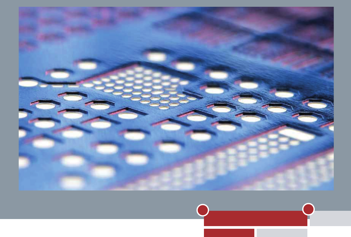
The whole solution chain from a single source
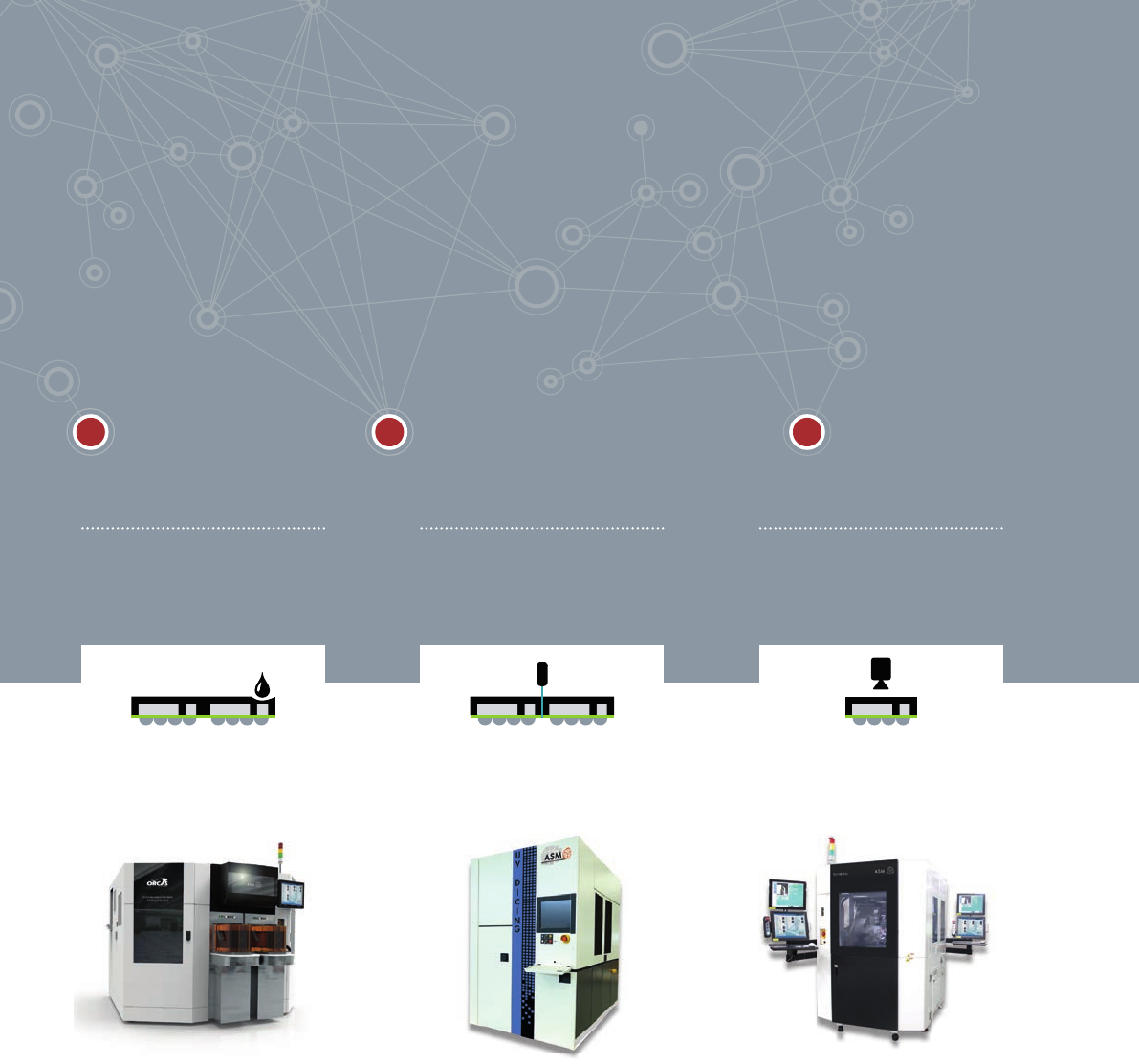
Wafer-level System-in-Package (SiP) Process
ENCAPSULATION
ORCAS
Flexible molding
SINGULATION
LASER 1205
Precise and efficient
laser-cutting
WLP INSPECTION,
TEST & PACKAGING
SUNBIRD
Highly efficient all-in-one
solution
Molding
Next, the substrates with the SiPs is mol-
ded, usually via press-forming with epoxy.
For these and the subsequent SiP process
steps such as redistribution layer in thin-
layer technology, proven tools from the
semiconductor industry is normally used,
which explains why most SiP processes
operate with wafer-shaped panels.
Singulation
In the singulation process, classic saws
have been replaced by laser-based solu-
tions, because they are faster and more
accurate. Even more modern solutions
already operate with multi-beam lasers.
From testing to taping
The SiP must be picked up, optically in-
spected, tested, sorted, marked, labeled,
and packaged in tapes for the placement
process. Modern solutions have turrets and
combine these steps in a single machine.
End-to-end solution chain
All of these steps form a multi-layered,
complex process that can only be managed
with a consistently coordinated solution
chain as well as with lots of experience and
competence. Only ASM can offer this solu-
tion chain from a single source. Check out
the following pages for more details.
5
Deposition
PrintingStencil technology
Die Attach & SMT
1
2
The assembly of ultra-compact SiP de-
signs requires maximum precision and
extremely thin stencils with ultra- ne
apertures. This is the only way to achieve
the area ratio parameters that permit a
reliable release of the print media and
ensure a stable printing process.
In addition, specially developed multi-layer
stencil technology is used to place solder
balls directly on the substrate. In a rst
step, ux is applied, which is important for
the soldering process. Next, the solder
balls for the SMT components are applied
in a second printing process. This would
be impossible without specially developed
multi-level stencils whose cavities leave
the ux deposits untouched.
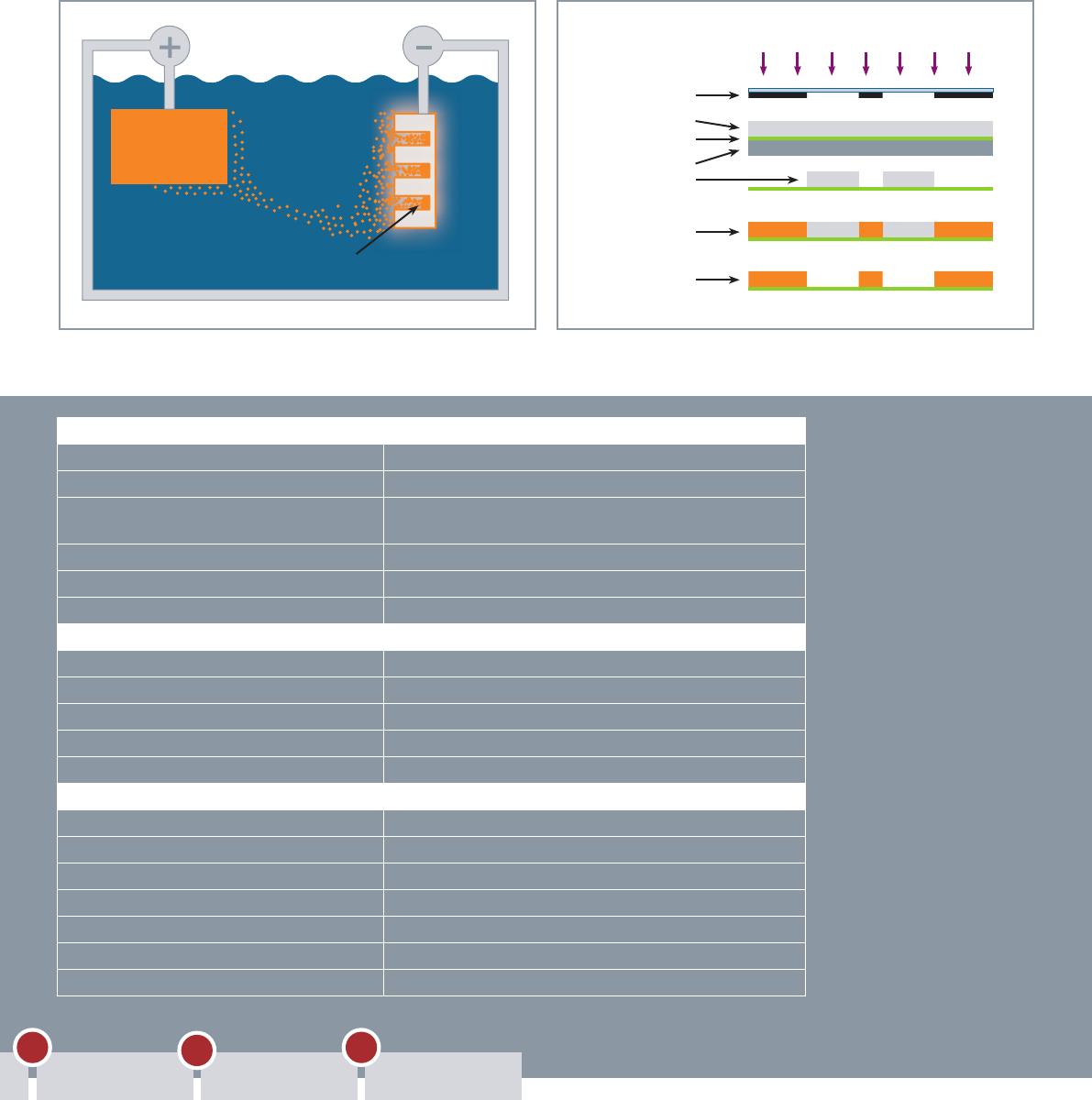
Classic etching or laser-cutting methods
quickly hit their limits with such stencils,
which is why ASM has for many years pu-
shed the development of electroforming as
an additive manufacturing method for high-
precision stencils. With a galvanic process
and supported by lithography, multi-level
stencils can be made from various materi-
als with tolerances in the nanometer range.
Another plus of DEK e-formed stencils is
the extremely high quality of their surfaces
and aperture walls, which makes for signi-
cantly improved printing media release
characteristics, more accurate paste de-
posits, and reduced understencil cleaning
frequencies.
In summary, the combination of DEK
E-Form high-precision stencils and DEK
printing solutions lets you manage your
printing process with ef ciency and relia-
bility.
Stencil Technology
E-forming produces the finest multi-level apertures
6
Die Attach & SMT
Encapsulation Singulation
WLP Inspection,
Text & Packing
3
4
5
ELECTROFORM STENCIL PRODUCTS SPECIFICATIONS
Platinum Stencil Product Range
Aperture (hole) size tolerance ±4 μm
Aperture positional tolerance distance < 50 mm ±50 µm
> 50 mm 0.1 µ/mm (VG) , 0.3 µ/mm (mesh mounted)
Thickness tolerance ±5 % of thickness
Fiducials max. 8
Material nickel 500 HV ±50
QC
Aperture checking 10 apertures
Thickness checking 5 × in Image area + coc
X/Y accuracy check + coc
Documentation extended + drawing
Scan (presence/absence) 100 %
RECOMMENDED PRINT APPLICATIONS
semiconductor packaging
wafer level printing
LED and/or trace printing
high accuracy printing
multi layer stencil
aperture sizes down to 25 µ
min. thickness possible 20 µ (0.75mil)
7
Mask
Photoresist
Seed layer
Substrate
Photoresist
molds
Electroformed
metals
Metallic
microstructure
Source: Wikipedia
UV Light or X-rays
Electrolytic solution Electroform
Electrodeposition
process
Metal