17-2756-ASM Broschüre ASM AP EN_171020 - 第8页
TRS T ooling Die Attach & SMT Deposition Printing Stencil technology 1 2 Advanced packaging places extremely high demands on the printing process, be- cause it requires ultra-ne apertures and maximum precision along…
Die Attach & SMT
Encapsulation Singulation
WLP Inspection,
Text & Packing
3
4
5
ELECTROFORM STENCIL PRODUCTS SPECIFICATIONS
Platinum Stencil Product Range
Aperture (hole) size tolerance ±4 μm
Aperture positional tolerance distance < 50 mm ±50 µm
> 50 mm 0.1 µ/mm (VG) , 0.3 µ/mm (mesh mounted)
Thickness tolerance ±5 % of thickness
Fiducials max. 8
Material nickel 500 HV ±50
QC
Aperture checking 10 apertures
Thickness checking 5 × in Image area + coc
X/Y accuracy check + coc
Documentation extended + drawing
Scan (presence/absence) 100 %
RECOMMENDED PRINT APPLICATIONS
semiconductor packaging
wafer level printing
LED and/or trace printing
high accuracy printing
multi layer stencil
aperture sizes down to 25 µ
min. thickness possible 20 µ (0.75mil)
7
Mask
Photoresist
Seed layer
Substrate
Photoresist
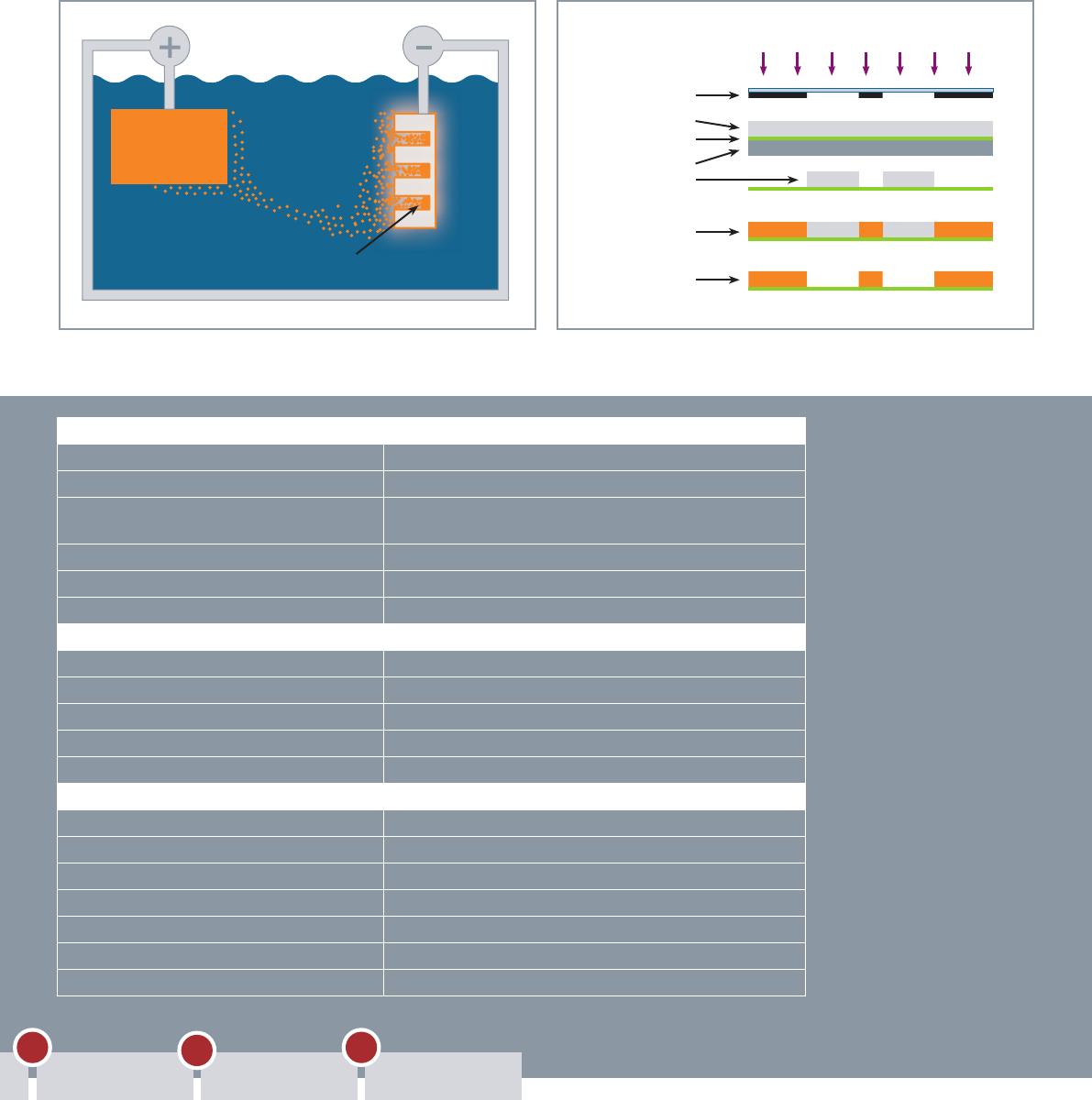
molds
Electroformed
metals
Metallic
microstructure
Source: Wikipedia
UV Light or X-rays
Electrolytic solution Electroform
Electrodeposition
process
Metal
TRS Tooling
Die Attach & SMTDeposition
PrintingStencil technology
1
2
Advanced packaging places extremely
high demands on the printing process, be-
cause it requires ultra-ne apertures and
maximum precision along with separate
printing steps involving different technolo-
gies and media.
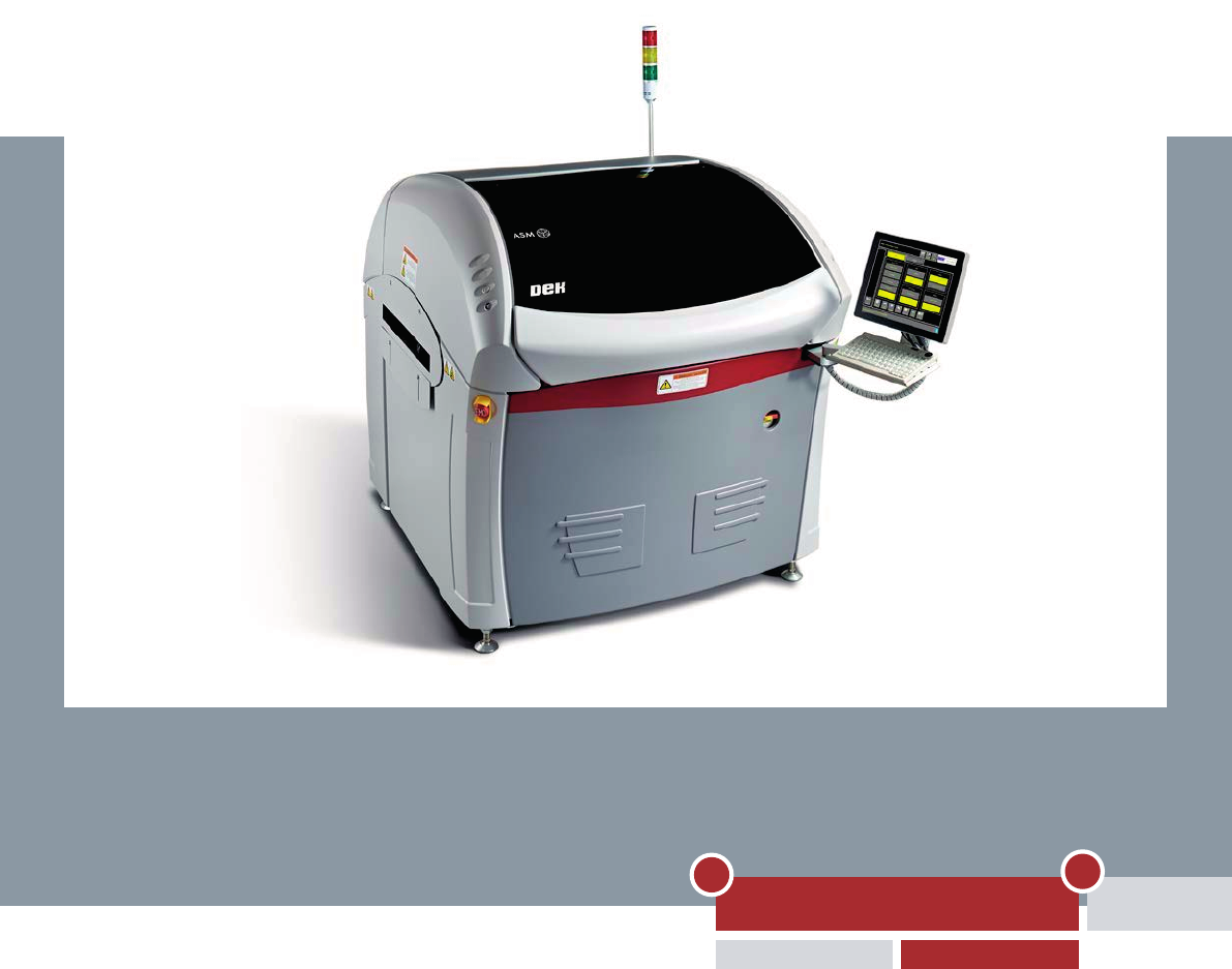
With the DEK Galaxy, our printing experts
have developed an extremely powerful,
modular and exibly congurable solution
for use in advanced-packaging processes.
Precise linear motors and a stable frame
ensure maximum precision even at high
printing speeds. In addition, ASM offers
a variety of options and accessories that
enable you to optimally adapt the DEK
Galaxy to your specic process require-
ments, starting with the conveyor, whose
standard version already accommodates a
wide range of panel sizes. Conveyor solu-
tions for high-precision (and heavy) wafer
carriers are also available.
A wide range of sensors and the
HawkEye
®
inspection system ensure
seamless process control. SMEMA- and
HERMES-compatible interfaces makes
it easy to integrate the machine into your
lines and processes.
Printing & Ball Drop
The printing solution for advanced packaging processes:
DEK Galaxy
8
TRS Tooling
TRS tooling
Flux printing
Die Attach & SMT Encapsulation Singulation
WLP Inspection,
Text & Packing
3
4
5
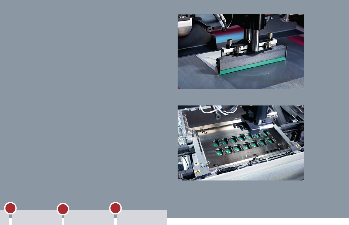
Flux and solder paste
With the rst two printing processes,
ux or solder paste are applied to the
substrates via classic stencil printing
with multi-level DEK e-form stencils.
The versatile DEK printer software ma-
kes it easy to adjust all relevant opera-
ting parameters.
Ball drop
For the ball drop process, i.e. the appli-
cation of solder balls onto the underside
of the SiPs, the DEK Galaxy provides
another solution. With its DirEKt Ball
Placement Option, solder balls can be
applied individually (ball attachment).
DEK Galaxy
Reliable printing in chip assembly
▪ For demanding wafer, substrate and circuit board
applications
▪ Process Alignment Capability: 2 Cpk @ ±12.5 µm 6 sigma
▪ ProFlow
®
DirEKt Imaging technologies for high-precision
ball placements
▪ Modular: Flexibly configurable with toolings and transport
systems for the widest range of advanced packaging
applications
▪ SMEMA- and HERMES-compatible interfaces to wafer
and flux solutions
▪ Fast: Core cycle time of only 7 seconds
▪ Flexible: Product changeovers take less than 2 minutes
▪ Easy to use: DEK Instinctiv™ software
9