1OM-1505-004_w.pdf - 第175页
1OM-1505 3. Specications of Printing Stencil Plate Making : Chap.5 5-24 (8.4) How to make a stencil recognition mark Method: • Engrave the stencil recognition mark by half-etching and bury epoxy resin adhesive mixed wit…

1OM-1505
3. Specications of Printing Stencil Plate Making : Chap.5
5-23
(8) Material of Stencil Plate and Setting of Stencil Recognition Mark
(8.1) Material of Stencil Plate
•
It is recommended that a metal mask made of stainless st
eel or full
additive Ni should be used.
•
The recognition may become unstable because the Cu-Ni
metal
mask has strong gloss on its surface.
Therefore, it is required to
reduce the gloss by delustering the mask surface (the range of 10 ×
10 mm around the center of the stencil recognition mark).
Note
The stencil recognition mark should make ample contrast with the
surroundings. (Prevention of False Recognition) When the mask
surface is honeycomb-processed, the area (10 × 10 mm around
the center of the stencil recognition mark) should not be processed
into a honeycomb type.
(8.2) Position of Stencil Recognition Mark
•
It is recommended that the stencil recognition mark be lo
cated at the
same position as the PCB Recognition mark on the PCB.
•
Use an etching positive
lm (a
lm used to make a stenci
l plate)
equivalent to the conductive land positive
lm (a le used to make a
PCB). (Improvement of Accuracy)
Note
Anything like a pattern similar to a stencil recognition mark
should not exist in the designated window.
(8.3) Shape of Stencil Recognition Mark
•
It is recommended that the shape of the stencil recognition mark be
the same as the PCB Recognition mark put on the PCB. A through
hole and a pad mark are excluded.
•
Refer to "Fiducial Marks" for the detailed information of the shape
and size of the stencil recognition mark.
1103-003
1OM-1505
3. Specications of Printing Stencil Plate Making : Chap.5
5-24
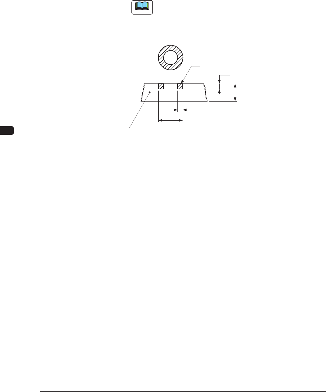
(8.4) How to make a stencil recognition mark
Method:
•
Engrave the stencil recognition mark by half-etching and bury epoxy
resin adhesive mixed with carbon powder into the grooves.
•
A
fter c
uring the adhesive, nish the surface of the stencil recognition
mark and the upper surface of the mask such that both surfaces
become flush. ( against the surface)
Note
A punched hole can be used as a stencil recognition mark if there
is no solder paste around the hole.
Example:
t / 2
Stencil Recongnition Mark
Stainless Metal Mask
1.0 to 2.0
0.35
t = 0.15 to 0.2
Unit : mm
F1E8
Reference Material:
•
Epoxy Resin/Sumitomo 3M/Base 1838B, Hardening Agent 18
38A
•
Carbon Powder/Nishimura Kokuen/Earthy Graphite, Particle Size 1.5
µm
0
-0.05
1103-002
1OM-1505
3. Specications of Printing Stencil Plate Making : Chap.5
5-25
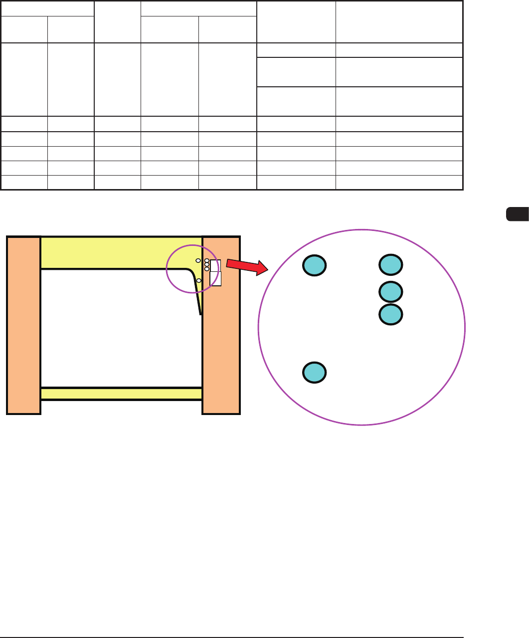
(9) The Range of PCB Width (Y Direction) in which Printing is Possible
Table "T1E7" shows the size of stencil frame and the applicable PCB on
which printing is possible according to the difference in the stencil plate
making reference.
For the PCB width (Y direction), the stopper pin can be positioned at
the rear, center or front according to the stencil frame size, plate making
reference and transfer reference.
Stencil Size Pin
Position
Max. Printable PCB Size
Plate Making
Reference
Paste Release Action
Restricted on the Rear Side
X
direction
Y
direction
X direction Y direction
750 750 A 510 460 Rear Not Available
Center 430 or more for PCB
Direction Y Not Available
Front 445 or more for PCB
Direction Y Not Available
736 736 B 490 381
Rear/Center/Front
None
720 720 C 470 381
Rear/Center/Front
None
750 650 E 510 381
Rear/Center/Front
None
650 750 D 330 381
Rear/Center/Front
None
650 550 E 330 250
Rear/Center/Front
None
Unit : mm
T1E7
A
B
C
D
E
F1E9
1103-002