1OM-1505-004_w.pdf - 第179页
1OM-1505 4. Fiducial Marks : Chap.5 5-28 (3) Material Copper Leaf, Nickel Plating, Solder-Plating, Solder Leveler, Gold Plating Note (a) A copper leaf, a resist, a coating, a silk print, and a punched hole should not exi…
1OM-1505
4. Fiducial Marks : Chap.5
5-27
T1E8-2
Note
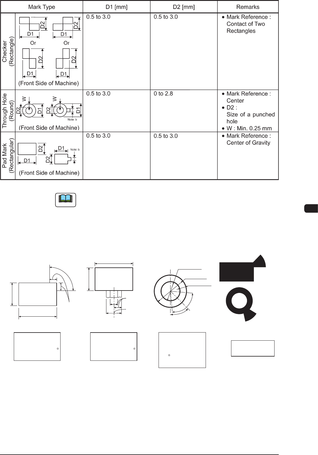
(a) The error of the mark size should be within ± 10% by comparison with the
reference pattern.
(b) A through hole or a pad mark should have only one land which is directed
in increments of 45°
(2) Specications of Line extended from a pad Mark or a Through Hole.
Range of Tangent
Lines related between
Pad Mark and Land
Range of Land
Location in
Increments of 45
for Pad Mark
(Front Side of Machine)
1/3 of Side
0.5 to 2.0
0.5 to 3.0
Examples of
Land Locations
0.5 to 2.0
0.5 to 3.0
0.5 to 1.5
1.0 to 3.0
Min.0.25
45°
80°
(Front Side of Machine)
(Front Side of Machine)
(Front Side of Machine)
Range of Land
Location in
Increments of 90
for Pad Mark
Range of Land
Location for
Through Hole
(45
at the bottom
right of the hole)
(Range of Tangent
Lines related between
Pad Mark and Land)
Range of Tangent
Lines related between
Pad Mark and Land
1/3 of Side
Unit : mm
F1E10
1103-003
1OM-1505
4. Fiducial Marks : Chap.5
5-28
(3) Material
Copper Leaf, Nickel Plating, Solder-Plating, Solder Leveler, Gold Plating
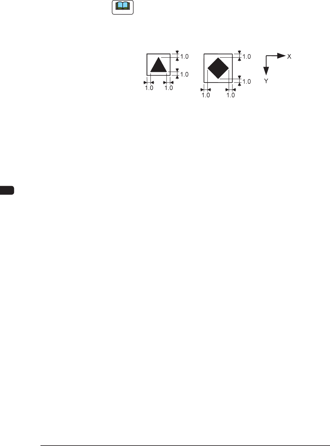
Note
(a) A copper leaf, a resist, a coating, a silk print, and a punched hole
should not exist in the range of 1.0 mm in both X and Y directions
from the outermost edges of a ducial mark. They may cause a false
recognition.
Example :
(Front Side of Machine)
Unit : mm
F1E11
(b) The shape of PCB (a cutout, a punched hole), the external elements
(light reflected from a structure, light emitted from an external device,
etc.) may sometimes interfere with recognition of ducial marks.
(c) A ducial mark should make ample contrast with the surroundings.
(To prevent false recognition)
(d) Anything resembling a pattern similar to a ducial mark should
not exist in the designated window. If one exists, it may cause false
recognition.
(e) A test may be required when the ducial mark cannot be recognized
because of the extreme warpage of the PCB.
1103-003
1OM-1505
5. Measured Noise Value : Chap.5
5-291103-002
5. Measured Noise Value
[Measurement Condition]
•
Measuring Position
Position 1 m away and 1.6 m in height from the machine (Both Front and Rear
Sides of Machine)
•
Noise Measuring Instrument
RION Model : NA-60
Results of Measurement:
Max. 68.0 [dB] (Measuring Point b) Background Noise:
40.0 [dB]
Requirements for
Machine Operation
Measured Noise Value [db]
Remarks
Normal Operation
Measuring Point a
67.2 [dB]
•
Temperature 25.5°C
Measuring Point b
65.0 [dB]
Measuring Point c
68.0 [dB]
Measuring Point d
65.8 [dB]
T1E9