1OM-1505-004_w.pdf - 第198页
1OM-1505 5. PCB Backup Jig (PCB Width W "50<=W<65") : Chap.6 6-15 5.3 V ariant Drawing for the Component Section (P/N 23-1). b b 4-C1 0.03 A A 0.03 Material : A5052 Processing : None 23-1 Engraved mark fo…
1OM-1505
6-14
5. PCB Backup Jig (PCB Width W "50<=W<65") : Chap.6
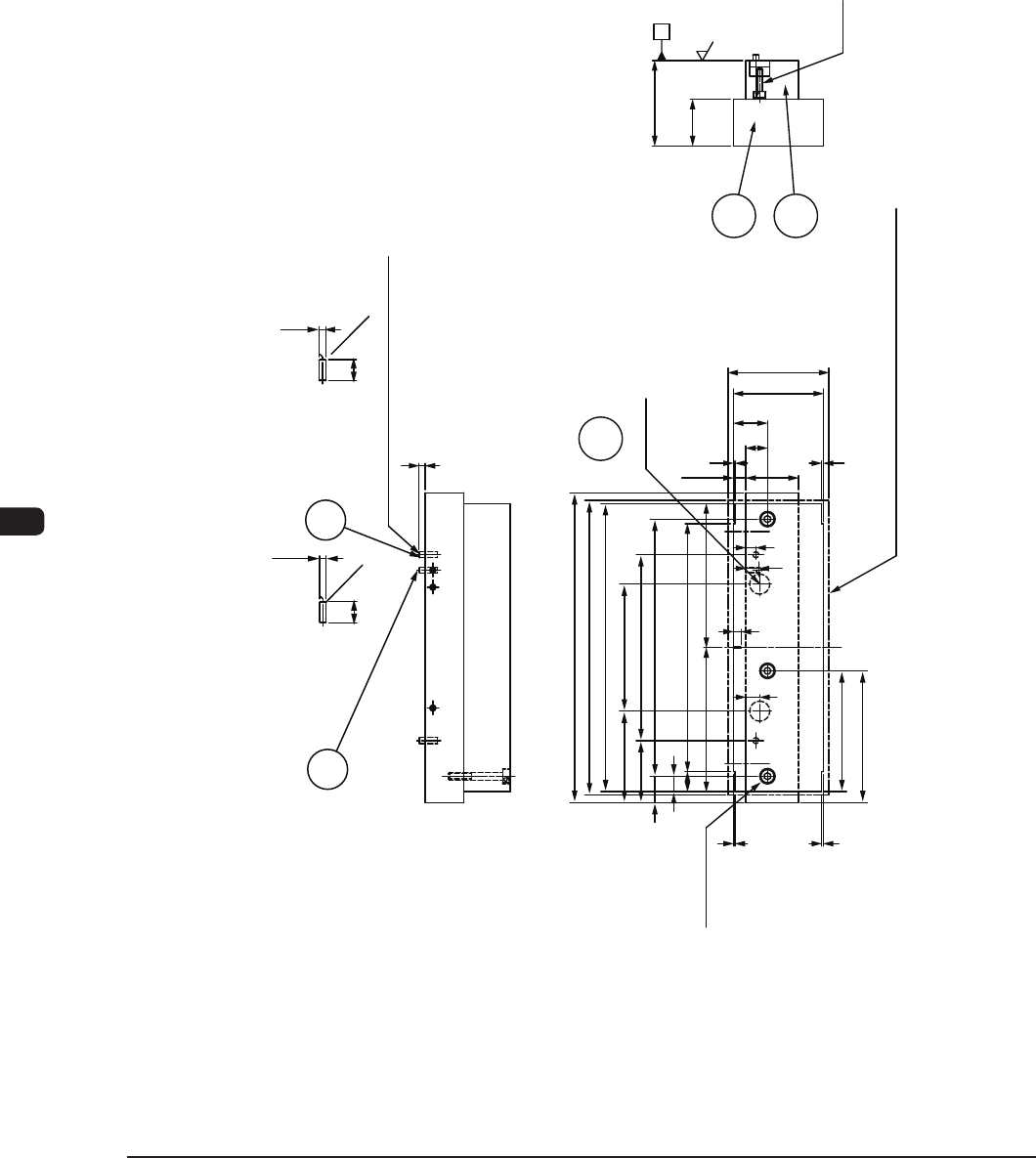
5.2 Assembly Diagram
Magnets
Q-M5L35
X2
S-1
*
23-2
23-1
2-M4L15
HXU13 (MISUMI)
4 4 4
1.6
R
Notes : (a) The part with the P/N S-1 is a part to be purchased.
(b) After assembling each component, process the R-surface so that
the * marked dimensions are met.
(c) The part with the P/N 21-4 and 21-5 are attached after
the processing of R-surface.
(d) The part No. 21-5 is not used for model PXH-1, TPM-100 series,
TPM-200 or TPM-5000.
4
11
A
L
L-4
TX
120±0.03
55±0.03
30
8±0.0534
6.5
8.5
5
9
14
22
W-7
W
11
S
D
E
R
C
G
L/2-2
U
Z
L/2-2
21-5
Positioning Pin (2 locations) Bonding with LOCTITE
21-4
2-C0.5
2-C0.5
F3.9g6
F3.6
0
-0.1
Material : SUS304
Processing : None
Material : SUS304
Processing : None
12
12
The two-dot chain line shows the state that the PCB is positioned.
Note d
F1F10
1103-001
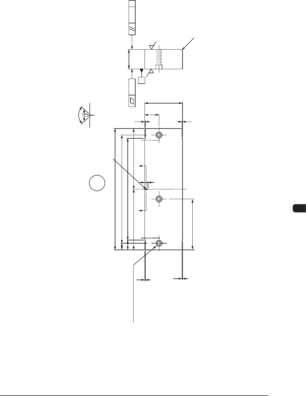
1OM-1505
5. PCB Backup Jig (PCB Width W "50<=W<65") : Chap.6
6-15
5.3 Variant Drawing for the Component Section (P/N 23-1).
bb
4-C1
0.03 A
A
0.03
Material : A5052
Processing : None
23-1
Engraved mark for center position
1.6
1.6
Q-F6 F9.5 Counterbore Depth 6
E
R
L/2-2
22
W-7
5
11
11
L/2-2
30
L-4
C
G
U
View b-b
90°
1
F1F11
1103-002
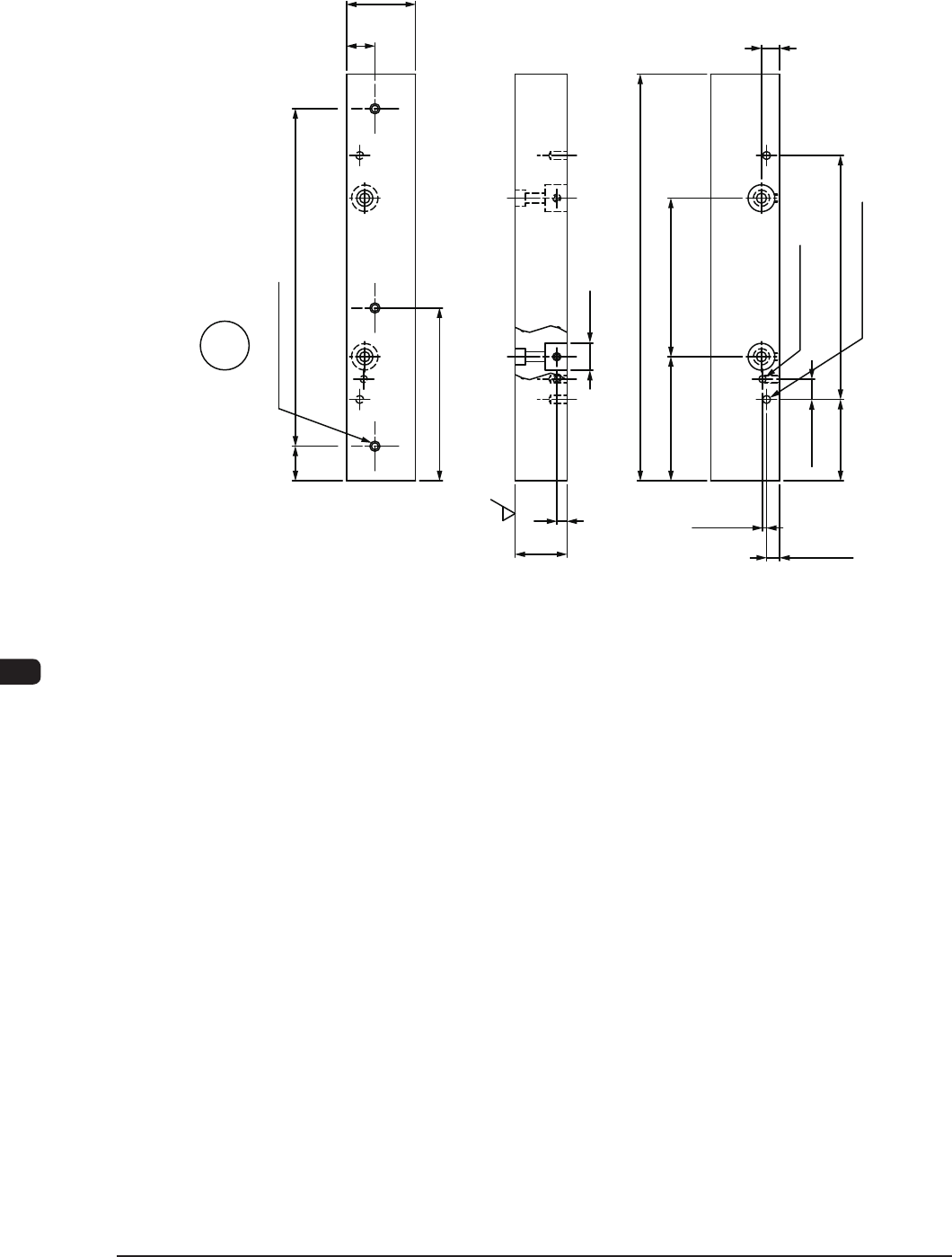
1OM-1505
6-16
5. PCB Backup Jig (PCB Width W "50<=W<65") : Chap.6
5.4 Variant Drawing for the Component Section (P/N 23-2).
Q-M5 Depth 15
D C
14
34
25.5
2±0.05
6.5±0.05
5
9
+0.3
0
2-13.2
A
TX
10±0.05
S 120±0.03
+0.2
0
F3.6 Depth 8
+0.1
0
2-F3.9 Depth 8
+0.03
0
Z
23-2
Material : A5052
Processing : None
1.6
F1F12
1103-002