2OM-1751-003w_G5S.pdf - 第136页
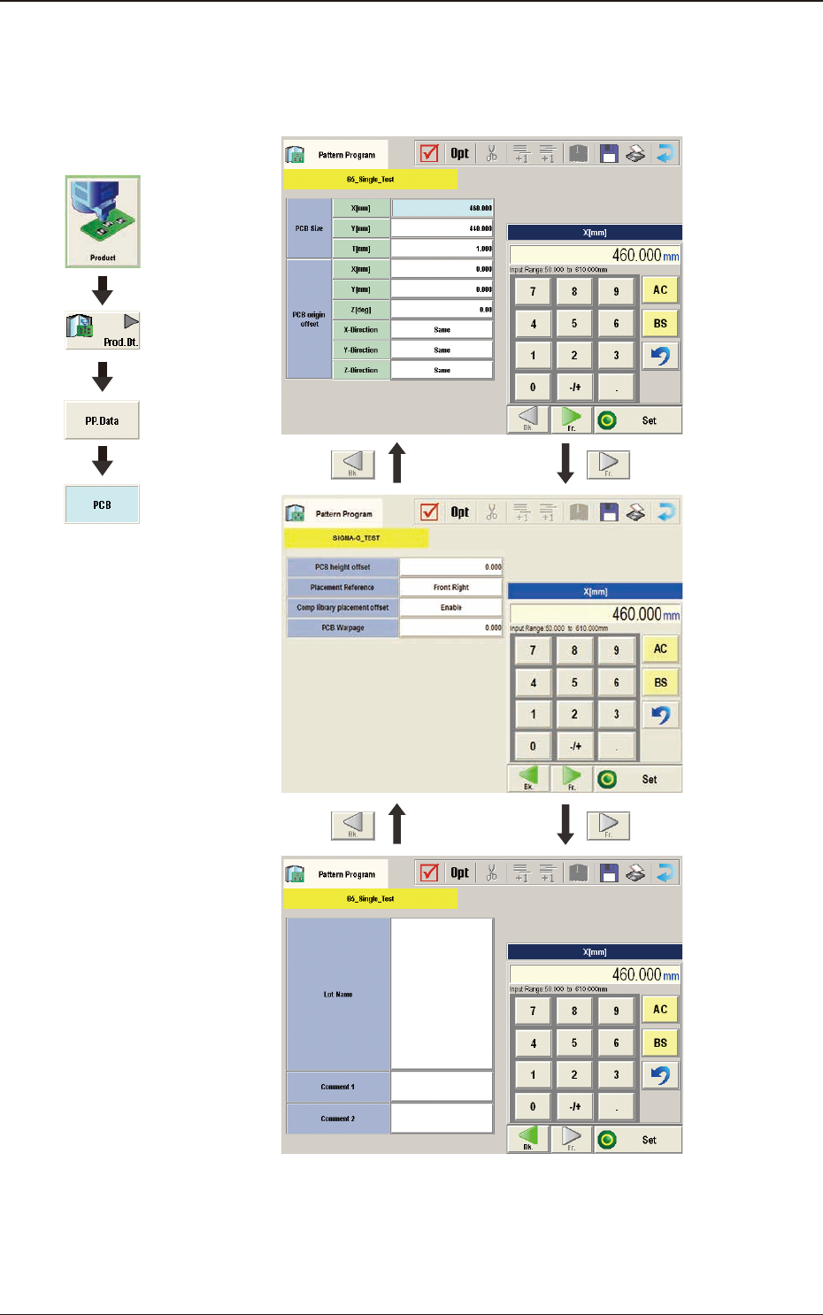
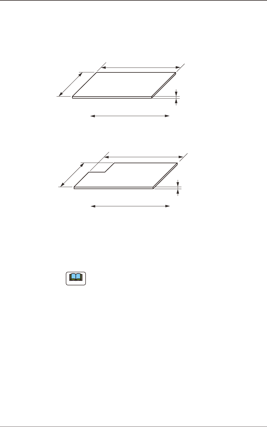
2OM-1751 2-14 1303-001 (B01_01) PCB size X (Horizontal), Y (V ertical), and T (thickness) [mm] Set the dimensions of the PCB to be produced. Y (V ertical) T (Thickness) PCB X (Horizontal) PCB Flow Direction F2B4 When the…
2OM-1751
2-13
3.2 PCB
(B01) PCB Data
F2B3
1303-001
Graphic
Development
3.2 PCB
2OM-1751
2-141303-001
(B01_01)
PCB size
X (Horizontal), Y (Vertical), and T (thickness) [mm]
Set the dimensions of the PCB to be produced.
Y (Vertical)
T (Thickness)
PCB
X (Horizontal)
PCB Flow Direction
F2B4
When the PCB has a cutout, the following dimensions must be entered.
Y (Vertical)
T (Thickness)
PCB
X (Horizontal)
PCB Flow Direction
F2B5
•
Data Input Range
X
: 50 to 610
Y
: 50 to 510
T
: 0.3 to 5.0
Note
(a) Be sure to set a correct parameter in the "X (Horizontal)" text
box because the set parameter is used to automatically correct the
placement position when a parameter is selected in the "PCB locate
method" text box in the "PCB transfer Mode Setup" tab sheet.
(b) The set parameter in the "Y (Horizontal)" text box must be used as a
target width for the conveyor width automatic adjustment operation.
(c) "T (Thickness)" is used as a target value for the backup table
ascending position when a PCB is clamped by the clamp plates and
positioned.
3.2 PCB
2OM-1751
2-151303-001
(B01_02)
PCB origin offset
X (Horizontal), Y (Vertical) [mm]
Set the offset values to correct the difference between the placement
coordinate reference (N0) and the PCB origin (P0).
"Plus" or "Minus" can be set in both X and Y coordinates in the direction of
the correction.
Placement Coordinate Reference Point :
For Front Right
Y
PCB Origin(P0)
PCB
X
Placement Coordinate Reference (N0)
PCB Origin(P0)
Y
X
Placement Coordinate Reference (N0)
X
Y
PCB
PCB Origin(P
0)
Placement Coordinate Reference (N0)
Y
X
PCB
PCB Origin(P
0)
Placement Coordinate Reference (N0)
Placement Coordinate Reference Point :
For Rear Left
Placement Coordinate Reference Point :
For Front Left
Placement Coordinate Reference Point :
For Rear Right
PCB
+
+
+
+
+
+
+
+
F2B6
3.2 PCB