ISM6636A&B_Rev1.10解密.pdf - 第10页
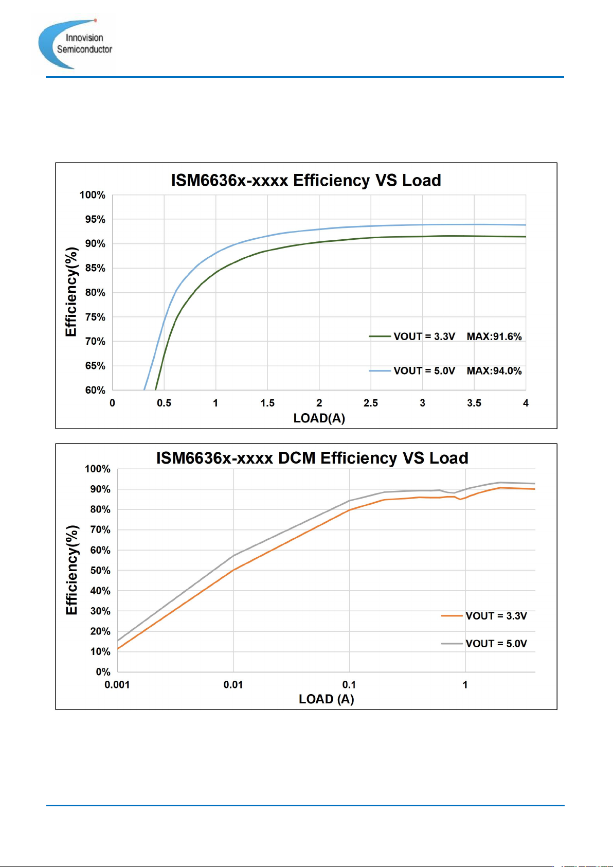
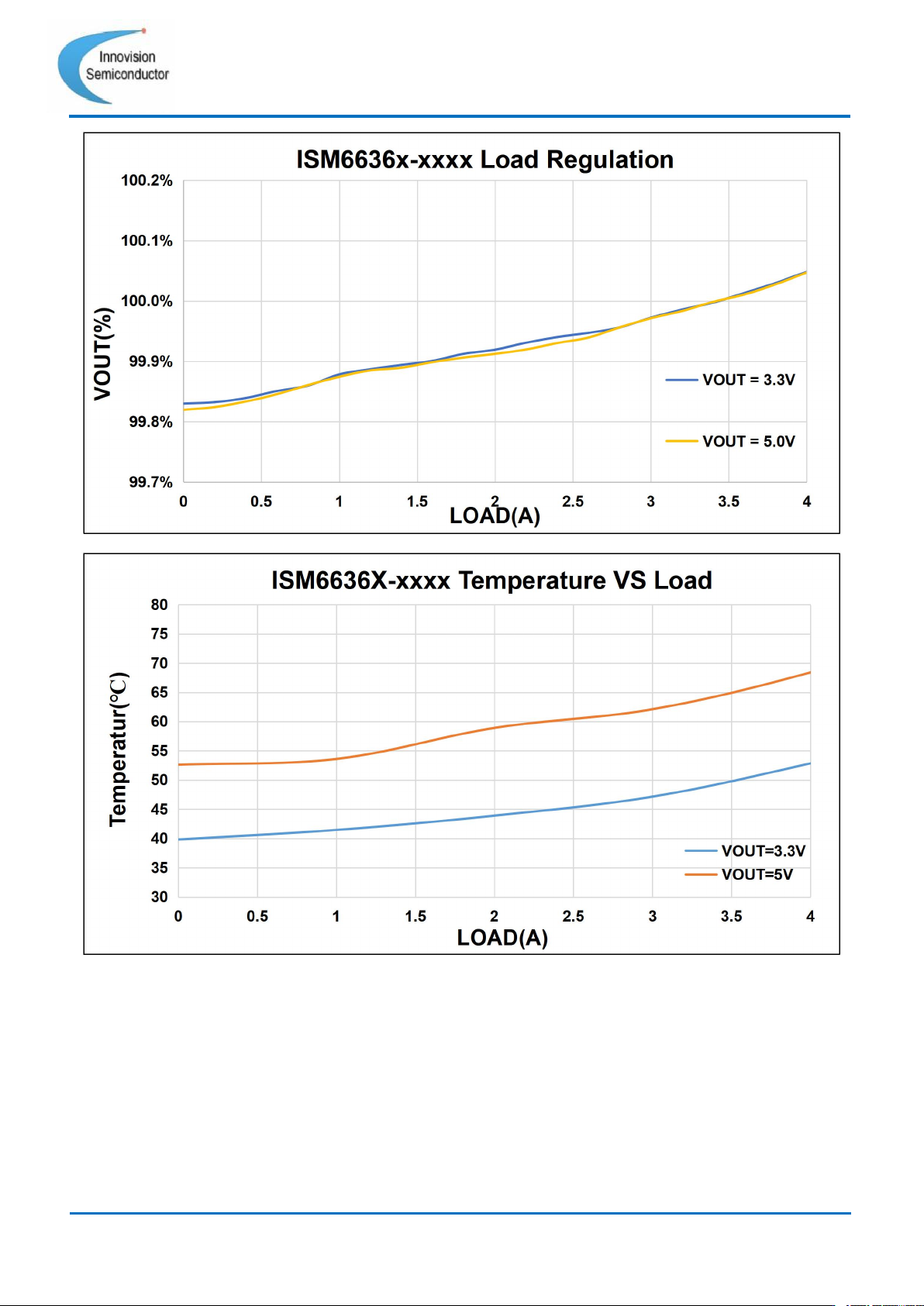
10 Innovision Semiconductor Preliminary Datas heet ISM6636 A/B Rev1.10 01/2023 Typical Perform ance Unless otherwise stated, sp ecifications apply over: P VIN = VIN = 12V,VOUT = 5 V,Typical values are specified at T A= 2…
9
Innovision Semiconductor
Preliminary Datasheet
ISM6636A/B
Rev1.10 01/2023
Unless otherwise stated, specifications apply over: 5V < PVIN = VIN< 16V, 0°C < TA <
125°C,Typical values are specified at TA= 25°C
I
2
C PARAMETER
CONDITIONS
(Note 2)
Fast-mode
Fast-mode plus
UNIT
MIN
MAX
MIN
MAX
T
OF
Output fall time
From V
IHmin
to
V
ILmax
20 × (VDD
/ 5.5 V)
250
20 × (VDD
/ 5.5 V)
125
ns
T
SP
Pulse width of spikes
that must be
suppressed by the
input filter
0
50
0
50
I
I
Input current each I/O
pin
PG = 0.5V, En =
2V
-10
10
-10
10
µA
C
I
Capacitance for each
I/O pin
10
10
pF
F
SCL
SCL clock frequency
0
400
0
1000
kHz
T
HD;STA
Hold time (repeated)
START condition
After this period,
the first clock
pulse is generated
0.6
0.26
µs
T
LOW
LOW period of the
SCL clock
1.3
0.5
T
HIGH
HIGH period of the
SCL clock
0.6
0.26
T
SU;STA
Set-up time for a
repeated START
condition
0.6
0.26
T
HD;DAT
Data hold time
I
2
C-bus devices
0
0
T
SU;DAT
Data set-up time
100
50
ns
T
R
Rise time of SDA and
SCL signals
20
300
120
T
F
Fall time of SDA and
SCL signals
20 × (VDD
/ 5.5 V)
300
20 × (VDD
/ 5.5 V)
120
T
SU;STO
Set-up time for STOP
condition
0.6
0.26
µs
T
BUF
Bus free time
between a STOP and
START condition
1.3
0.5
C
B
Capacitive load for
each bus line
400
550
pF
T
VD;DAT
Data valid time
0.9
0.45
µs
T
VD;ACK
Data valid
acknowledge time
0.9
0.45
V
NL
Noise margin at the
LOW level
For each
connected device,
including
hysteresis
0.1VDD
0.1VDD
V
V
NH
Noise margin at the
HIGH level
0.2VDD
0.2VDD
T
TO
SDA timeout
200
200
µs
Note 2. Guaranteed by design but not tested in production.