ISM6636A&B_Rev1.10解密.pdf - 第14页
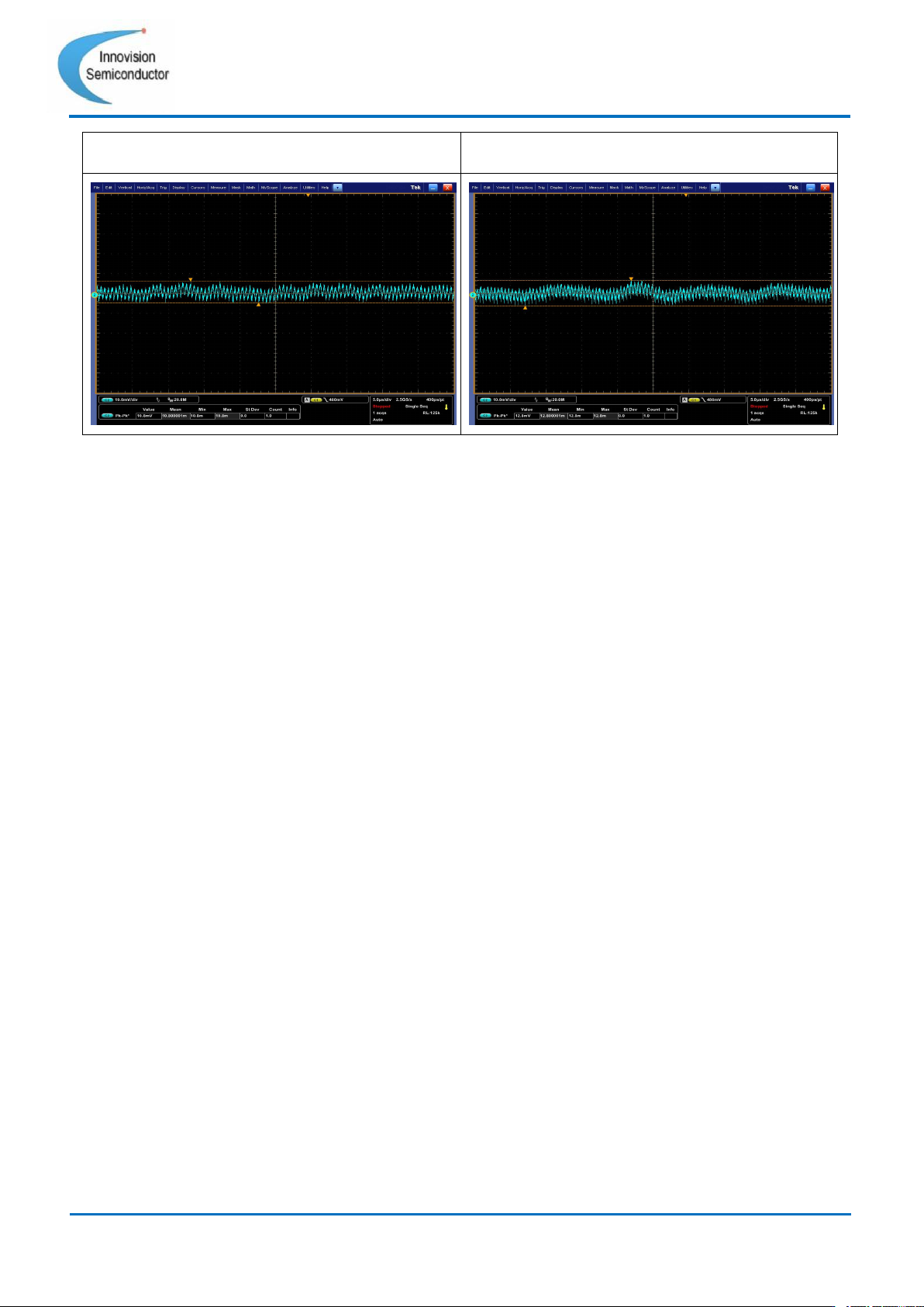
14 Innovision Semiconductor Preliminary Datas heet ISM6636 A/B Rev1.10 01/2023 VOUT Ripple LOAD = 0A CVOUT = 44μF VOUT Ripple LOAD = 4A CVOUT = 44μ F

15
Innovision Semiconductor
Preliminary Datasheet
ISM6636A/B
Rev1.10 01/2023
Functional Description
Overview
The ISM6636A/B is a family of small size,
low current, and high performance power
modules. It integrates output inductor and
capacitors for a complete system solution.
For ease of use, the module utilizes I2C
digital design to optimize power supply
parameters. The control topology allows no
external loop compensation while providing
fast transient response. Additional output
capacitors can be added for each rail
without any loop stability issue.
LDO Voltage
The ISM6636A/B uses an internal LDO
(Low Drop-Out) regulator to provide stable
bias voltage for the internal circuitries. The
nominal voltage of this LDO is 5V. This
device also supports external bias voltage
applications. If the external bias voltage is
used, the VIN pin and VCC pin should be
connected together to bypass the LDO. If
an single rail operation is desired, the VIN
pin must be connected to the PVIN pin.
When the supply voltage is above UVLO
threshold, the device is enabled regardless
of the configuration.
I2C Operation
The ISM6636A/B adopts the I2C digital
protocol to provide direct communication
between the device and the outside system.
The I2C communication begins as soon as
when VCC_UVLO start threshold is
exceeded, memory register is fully loaded,
the supply initialization is finished and the
address offset is fully read. The default
base address is 0x08. The offset 0-3 is then
determined by connecting ADDR pins to
AGND pins either directly or through a
resistor. The address detector reads the
resistance of the connection at startup and
uses it to set the offset. This offset is then
added to the base I2C address to set the
address with which the master device will
communicate.
To choose an offset from 0 to 3, follow the
instructions below.
• 0 – 0Ω (short ADDR to AGND) (0000
1000)
• +1 – 10kΩ (0000 1001)
• +2 – 20kΩ (0000 1010)
• +3 – >30.1kΩ (0000 1011)
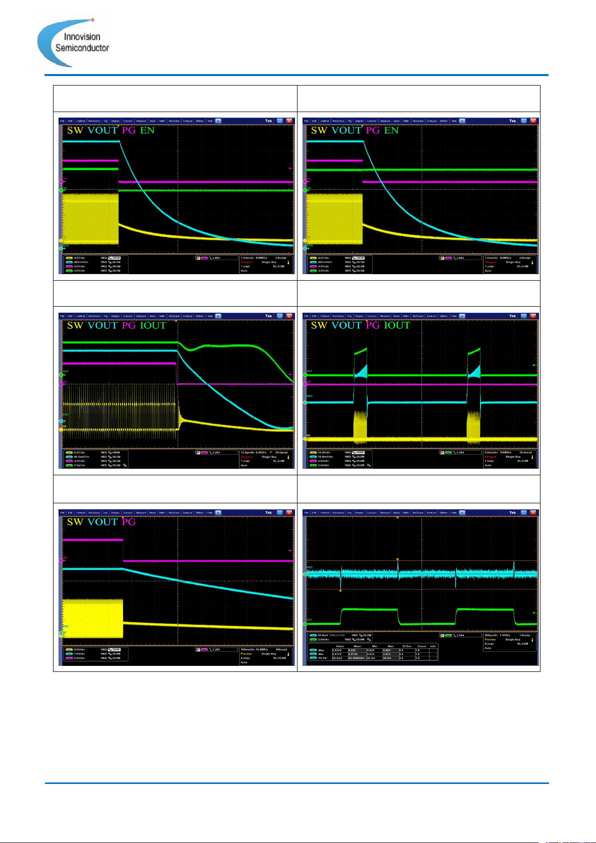
Soft-start Operation
The ISM6636A/B is designed to support a
smooth startup function with linearized
output voltage. This is accomplished by an
internal digital softstart circuit. When the
VCC exceeds the UVLO start threshold, the
loading of the contents of the non-volatile
memory into working register and
computing the address offset starts.
After the initialization is finished, Enable
(EN) pin is asserted (see Figure 1), the
internal reference voltage is soft-started to
the final target voltage level. The rate of
softstart is determined by the user register
bit SS_rate (see Table 1 below).
Register
Bits
Name/Description
0x14
[4:3]
SS_Rate:
00: 1mV/us, 01: 2mV/us
10: 0.5mV/us, 11: 4mV/us
Table 1 SS_Rate Register Description
During the initial softstart, the ISM6636A/B
uses minimum on time until the output
voltage rises. On time increases until VOUT
reaches the target value defined by the