ISM6636A&B_Rev1.10解密.pdf - 第26页
26 Innovision Semiconductor Preliminary Datas heet ISM6636 A/B Rev1.10 01/2023 Register = 0x0F Module temperature report (Temp_Rep ort) When the VIN pin is working normally, th e temperature information o f the m odule c…
25
Innovision Semiconductor
Preliminary Datasheet
ISM6636A/B
Rev1.10 01/2023
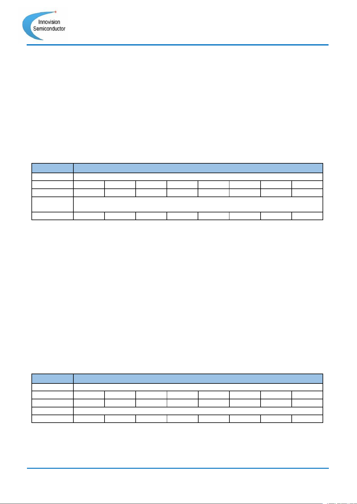
Register = 0x0D Output Voltage Report (Vout_Report)
When the VIN pin is working normally, the output voltage information can be read through
the I2C protocol. The output voltage of this register is related to the mantissa X of the read
range of ISM6636X.
When the part number is ISM6636A or ISM6636B, the output voltage reading range is
0.8~5.7V, LSB=20mV. The formula is as follows:
Vout =
V
Example (ISM6636B): When the read I2C value is 0x8C.
Vout =
V
Command
Vout_Report
Format
unsigned binary
Bit
7
6
5
4
3
2
1
0
Access
R
R
R
R
R
R
R
R
Function
ISM6636A\B Range:0.8V-->5.7V, 20mV resolution.
Default
0
0
0
0
0
0
0
0
Table 12 Register = 0x0D
Register = 0x0E Output current report (Iout_Report)
When the VIN pin is working normally, the output current information can be read through
the I2C protocol. The current can be read in the range of 0A~8.2A, LSB=40mA. There is a
constant offset in reading current information, and the calculation formula can be referred to
as follows:
.
Example: When the read I2C value is 0x72, 0x72=Dec(114)=114*0.04-2.5=2.06A. It means
the current output current is 2.06A.
When the read current exceeds 8.2A, the data fed back by the I2C is either the maximum
value. The output current information is for reference only. It is recommended that the user
read the current range as 0~6A. For accurate current information, also measure with an
external measuring instrument.
Command
Iout_Report
Format
unsigned binary
Bit
7
6
5
4
3
2
1
0
Access
R
R
R
R
R
R
R
R
Function
Iout Range: 0A-->8.2A, LSB= 40mA
Default
0
0
0
0
0
0
0
0
Table 13 Register = 0x0E
26
Innovision Semiconductor
Preliminary Datasheet
ISM6636A/B
Rev1.10 01/2023
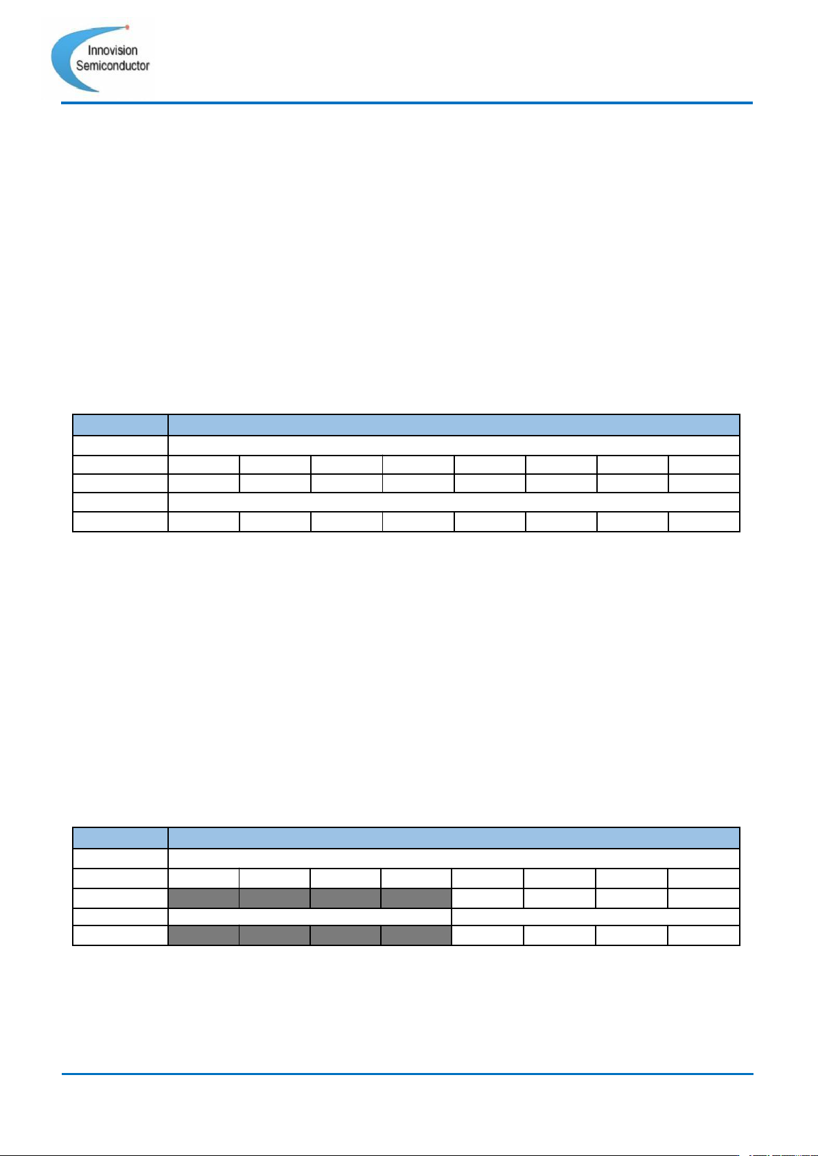
Register = 0x0F Module temperature report (Temp_Report)
When the VIN pin is working normally, the temperature information of the module can be
read through the I2C protocol. Temperature readable range is: -40°C~180°C.
LSB=1°C. There is a constant offset in reading temperature information. The calculation
formula can be referred to as follows:
5
Example 1:When the read I2C value is 0x65, 0x65=Dec(101)=101*1-75=26°C. Indicates the
module temperature 26°C.
The reading of temperature information will have a certain offset according to different
usage scenarios, but the maximum deviation will not exceed
±
10°C.
Command
Temp_Report
Format
unsigned binary
Bit
7
6
5
4
3
2
1
0
Access
R
R
R
R
R
R
R
R
Function
Range: -40°C--180°C, LSB=1°C.
Default
0
0
0
0
0
0
0
0
Table 14 Register = 0x0F
Register = 0x11 Ramp compensation amplitude setting (Ramp_Amplitude)
The ISM6636X provides an adjustable ramp compensation (Ramp) setting function. 0x00
indicates the minimum ramp compensation amplitude, 0xFF indicates the maximum ramp
compensation amplitude, and the amplitude increases as the bit increases. The ramp
compensation amplitude will affect the output load transient response (Load transient) and
frequency jitter (Jitter) of the module. When the ramp compensation amplitude increases,
the load transient response may become worse, but the jitter will become better. When the
ramp compensation amplitude is reduced, the load transient response (Load transient) will
be better, but the jitter (Jitter) will be worse. If the factory default settings can meet the
application requirements of the user's load transient response, it is recommended that the
default value is to be used.
Command
Ramp_Amplitude
Format
unsigned binary
Bit
7
6
5
4
3
2
1
0
Access
R
R
R
R
R/W
R/W
R/W
R/W
Function
no use
Adjust compensation ramp
Default
0
0
0
0
1
1
1
1
Table 15 Register = 0x11
27
Innovision Semiconductor
Preliminary Datasheet
ISM6636A/B
Rev1.10 01/2023
Register = 0x12 Set Vout voltage
Register = 0x13 Set Vout voltage
Register 0x12 and 0x13 need to be used together to implement the VOUT voltage setting
function. For ISM6636A/B, LSB = 10mV/Step. Register 0x12 Bit[0] and register 0x13 Bit[7:0]
form 9 bits with a total of 512 bits, which are used to set the output voltage.
These two registers will set the default value of the output voltage when the module leaves
the factory, as shown in the following table (16).
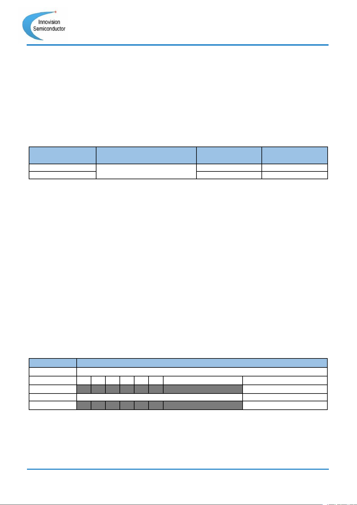
Base Part
Numbers
Package
Output
voltages(V)
Part Numbers
ISM6636B
LGA3.3X3.3-14L(P0.55T1.45)
3.30
ISM6636B-3300
ISM6636A
5.00
ISM6636A-5000
Table 16 ISM6636X part number table
ISM6636A\B output voltage is fixed at 5V\3.3V.
The user can adjust the output voltage in a small range.When modifying the voltage, you
must first write register 0x13 Bit[7:0] and then write register 0x12 Bit[0], the output voltage
command will take effect.
The output voltage calculation formula is as follows:
For ISM6636A/B,
the output voltage = ((Vout_high_bit * 256) + Vout_low_byte)* 0.01V + 0.8V.
Example: ISM6636A-5000 LSB=10mV/Step. Read register 0x12 Bit[0]=1, register 0x13
value is 0xA4. Converted to binary, it is Vout Bit[8:0]=110100100, which is calculated as
follows according to the formula:
Now need to modify the output voltage to 5.1V. The sequence needs to be followed, 1.
Write 0xAE to register 0x13. 2. Write 0B to 0x12[0]. When register 0x12[0] is written, the
command takes effect and the output voltage is modified to 5.1V.
Command
Vout_High_Bit
Format
unsigned binary
Bit
7
6
5
4
3
2
1
0
Access
R
R
R
R
R
R
R/W
R/W
Function
no use
Set up Vout voltage.
Default
0
0
0
0
0
0
\
Default
Table 17 Register = 0x12