ISM6636A&B_Rev1.10解密.pdf - 第3页
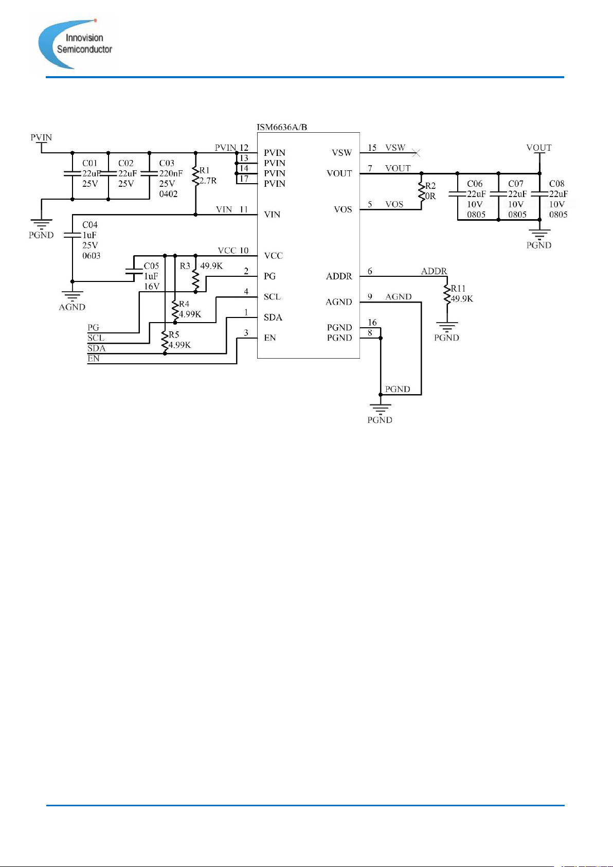
3 Innovision Semiconductor Preliminary Datas heet ISM6636 A/B Rev1.10 01/2023 Order Informat ion Base Part Numbers Package Outpu t voltages( V) Part Numbers Shipping Method ISM6636B LGA3.3X3.3- 14L(P0.55T 1.45) 3.3 ISM66…
3
Innovision Semiconductor
Preliminary Datasheet
ISM6636A/B
Rev1.10 01/2023
Order Information
Base Part
Numbers
Package
Output
voltages(V)
Part Numbers
Shipping
Method
ISM6636B
LGA3.3X3.3-
14L(P0.55T1.45)
3.3
ISM6636B-3300
3000
(Tape & reel)
ISM6636A
5.0
ISM6636A-5000
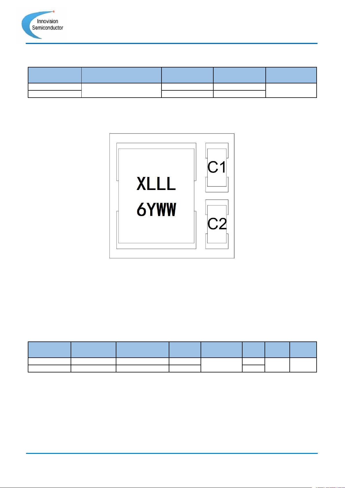
TOP MARKING (ISM6636A/B)
Top View
X:Base Part Number prefix
LLL : Last three digits of Lot Number
6: Indicate Part Number.
Y: Year code,for example, Y=1 indicates the year 2021
W: Week code
Base Part
Numbers
Output
voltages(V)
Part Numbers
x
LLL
6
Y
WW
ISM6636B
3.3
ISM6636B-3300
B
Last three digits
of Lot Number
B
Year
code
Week
code
ISM6636A
5.0
ISM6636A-5000
A
A
4
Innovision Semiconductor
Preliminary Datasheet
ISM6636A/B
Rev1.10 01/2023
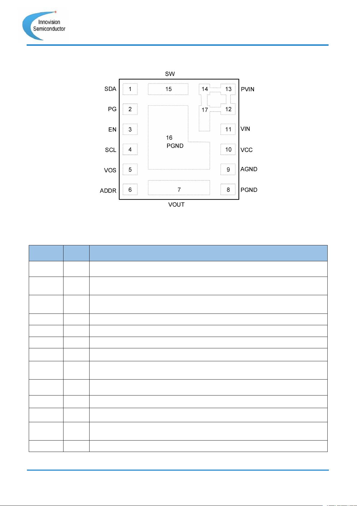
Package Reference
Top View
Pin Out Description
Pin
Name
Description
1
SDA
I2C Data Serial/Input/Output. Pull up to supply voltage with a 4.99k resistor.
2
PG
Power good output with open drain. If the output voltage is within regulation, the pull-up
resistor is required to indicate high.
3
EN
Enable pin. An input signal turns the regulator on or off. Connect EN to VIN through a
pull-up resistor. Do not float this pin.
4
SCL
I2C Clock. Pull up to supply voltage with a 4.99k resistor.
5
VOS
Output remote sense feedback.
6
ADDR
Address. Connect to AGND via a resistor to program I2C device address.
7
VOUT
Regulator output voltage. Place output capacitors between this pin and PGND.
8, 16
PGND
System ground. PGND is power ground of the power stage. Make the connection with
wide PCB traces.
9
AGND
Analog ground. Serves as the ground for internal reference and control circuitry.
10
VCC
Internal 5V LDO output. Supply power for the drive and control circuits.
11
VIN
Input voltage pin. Input for the internal LDO regulator.
12, 13,
14, 17
PVIN
Input voltage pin. Input for the internal MOSFETs.
15
SW
Test point for internal switch node. Connect to an isolated pad on the PCB.