ISM6636A&B_Rev1.10解密.pdf - 第6页
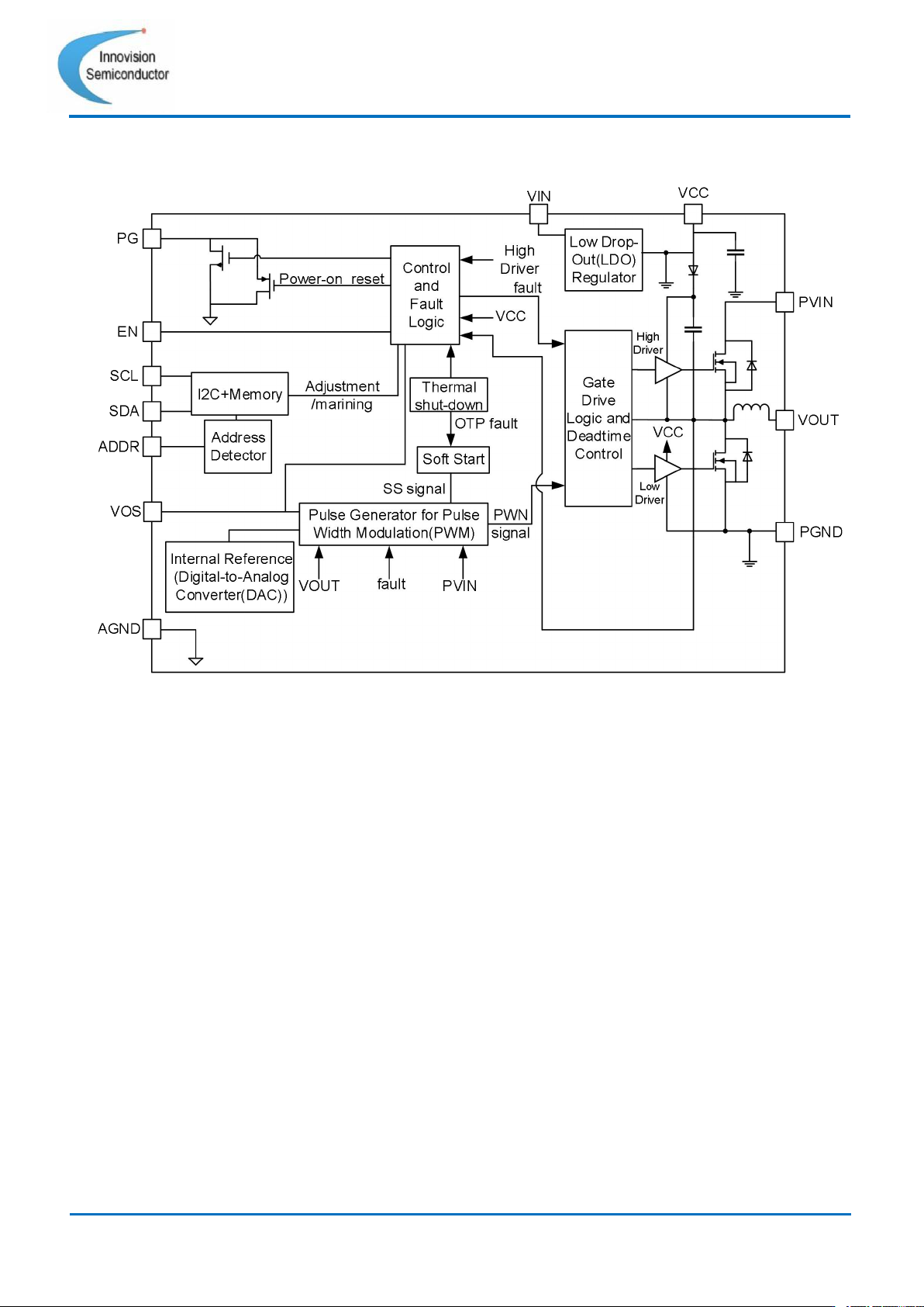
6 Innovision Semiconductor Preliminary Datas heet ISM6636 A/B Rev1.10 01/2023 Functional Block Diagram
5
Innovision Semiconductor
Preliminary Datasheet
ISM6636A/B
Rev1.10 01/2023
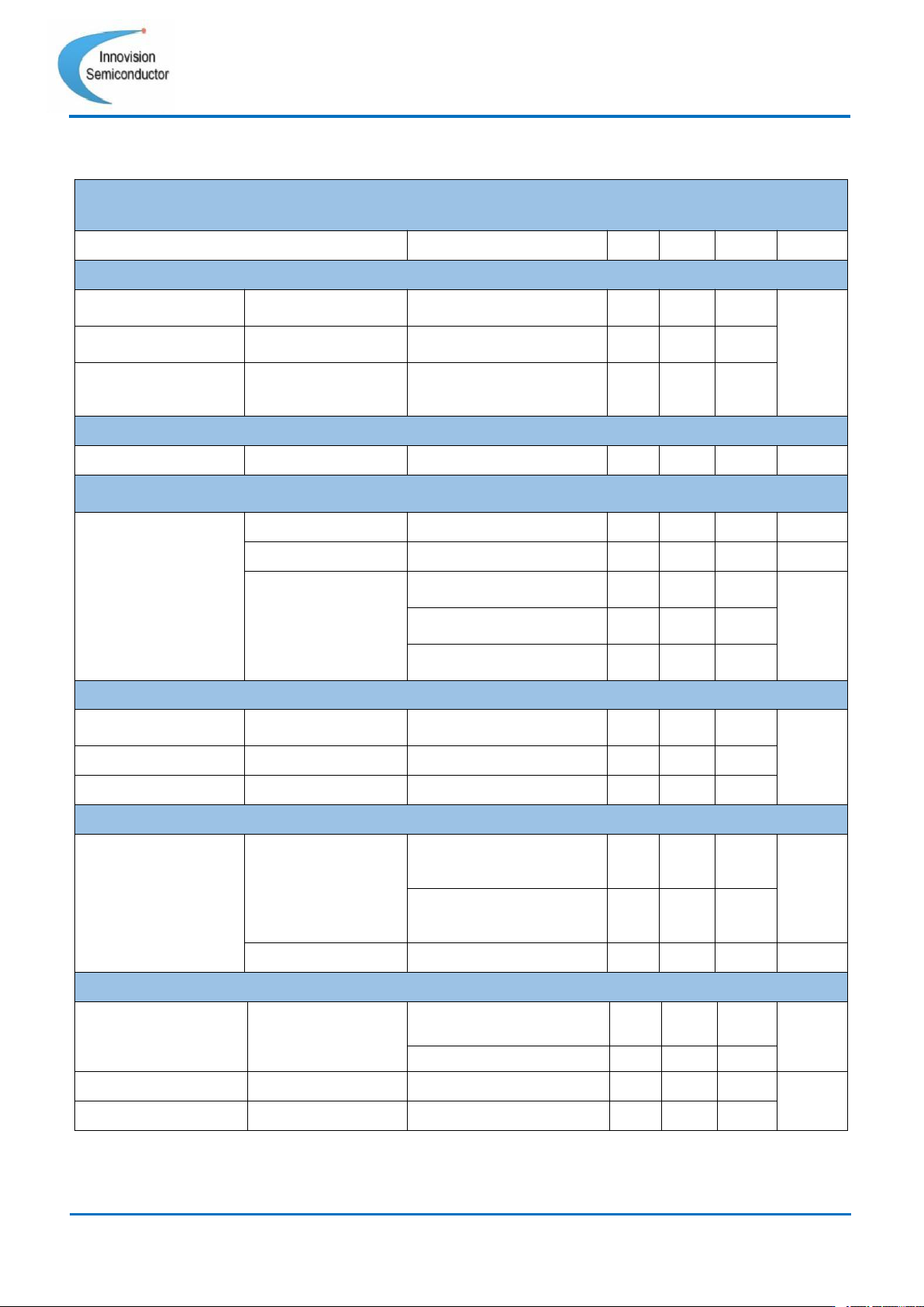
Absolute Maximum Ratings
PVIN to PGND…………….... -0.3V to 18V
VIN to PGND……………...… -0.3V to 18V
EN to PGND..………...………. -0.3V to 18V
SW to PGND
(
25ns
)
....…….....-5V to 23V
VCC to PGND….…….………-0.3V to 5.5V
VOS to AGND………..………-0.3V to VCC
All other pin to AGND .............-0.3V to 5.5V
PG to AGND…………..………-0.3V to VCC
PGND to AGND………..……-0.3V to +0.3V
Junction Temperature(Tj)…...……….150°C
Storage Temperature……...-65°C to 150°C
Recommended Operating
Conditions
Supply Voltage (VIN, PVIN)…5V to 16V
Bias Supply Voltage (VCC)…4.5V to 5.5V
Output Voltage (ISM6636B)……………3.3V
Output Voltage (ISM6636A)…………..…5V
Max Output Current (Io_max)………..… 4A
Junction Temperature (Tj).. -40°C to 125°C
Thermal Ratings
ΘJA Max....................................... 29 °C/W
ΘJB Typ (Still Air, No Heat sink).....5.1°C/W
Note 1. Stresses beyond those listed under “Absolute Maximum Ratings” may cause permanent damage to the device. These are stress
ratings only; functional operation of the device at these or any other conditions beyond those indicated in the operational sections of the
specifications is not implied. Exposure to absolute maximum rating conditions for extended periods may affect device reliabilit.
ESD Ratings
Electrostatic Discharge
Standard
Value
Human Body Mode (HBM)
JEDEC EIA/JESD22-A114
±2000V
Charge Device Mode (CDM)
JEDEC EIA/JESD22-C101F
±2000V
1). JEDEC document JEP155 states that 500-V HBM allows safe manufacturing with a standard ESD control process.
2). JEDEC document JEP157 states that 250-V CDM allows safe manufacturing with a standard ESD control process.
7
Innovision Semiconductor
Preliminary Datasheet
ISM6636A/B
Rev1.10 01/2023
Electrical Characteristics
Unless otherwise stated, specifications apply over: 5V < PVIN = VIN< 16V, 0°C < TA <
125°C,Typical values are specified at TA= 25°C
PARAMETER
CONDITIONS
MIN
TYP
MAX
UNIT
Supply Current
I
IN
(STANDBY)
VIN Supply Current
(Standby)
Enable low
1
mA
I
IN
(STATIC)
VIN Supply Current
(Static)
No switching, EN = 2V
2.3
I
IN
(DYN)
VIN Supply Current
(Dynamic)
EN high, VIN = 12V, V
OUT
= 5.0V, F
SW
=
1.875MHz(Note 2)
23
Soft-Start
SS
VOS Soft-Start Rate
Default
1
V/ms
Output Voltage
VOUT
VOUT (default)
5
V
Resolution
10
mV
Accuracy
Tj= 25°C, PVIN = 12V,
VOUT = 5V
±0.5
%
25°C< Tj< 125°C, PVIN =
12V, VOUT= 3.3V
-1
1
25°C< Tj< 125°C, PVIN =
12V, VOUT= 5V
-1.2
1.2
On-Time Timer Control
T
ON
On Time
PVIN = 12V, VOUT = 5V,
FSW = 1.875MHz
222
ns
T
ON
(MIN)
Minimum On-Time
(Note 2)
40
T
OFF
(MIN)
Minimum Off-Time
(Note 2)
184
SW Frequency
Fsw
SW Frequency
PVIN = 12V, VOUT =
3.3V, VOS connect to
VOUT.
1.875
MHz
PVIN = 12V, VOUT =
5.0V, VOS connect to
VOUT.
1.875
Accuracy
-15
+15
%
Internal Low Drop-Out (LDO) Regulator
VCC
LDO Regulator
Output Voltage
5.5V < VIN ≤ 16V, 0 -
20mA
4.8
5
5.2
V
5 ≤ VIN< 5.5V, 0 - 20mA
4.3
VLN
Line Regulation
5.5V < VIN ≤ 16V, 20mA
200
mV
VLD
Load Regulation
VIN = 12V, 0 - 20mA
100