ISM6636A&B_Rev1.10解密.pdf - 第7页
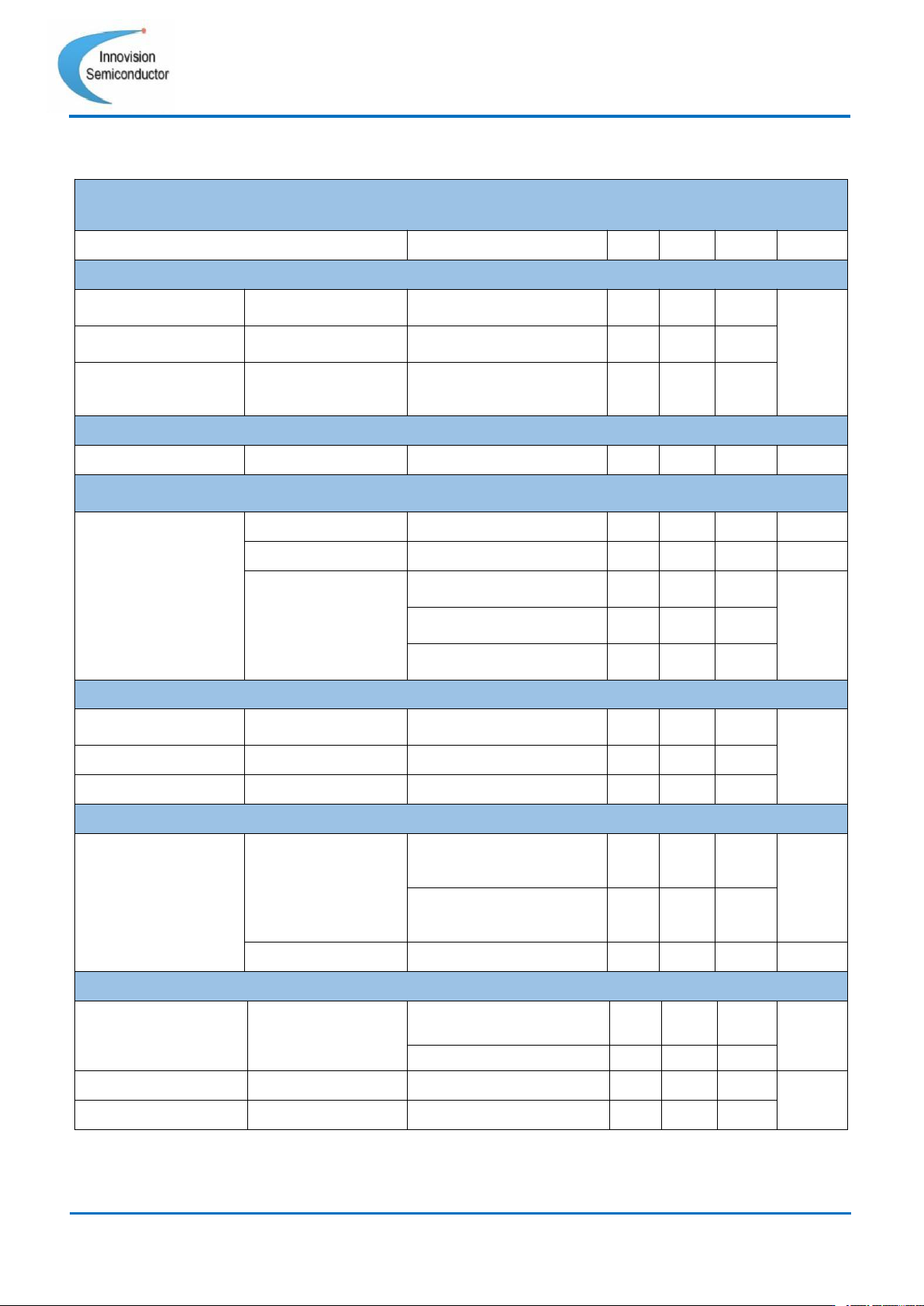
7 Innovision Semiconductor Preliminary Datas heet ISM6636 A/B Rev1.10 01/2023 Electrical Charac teristic s Unless otherwise stated, s pecifications apply over: 5V < P VIN = VIN< 16V, 0°C < TA < 125°C,Ty pic a…
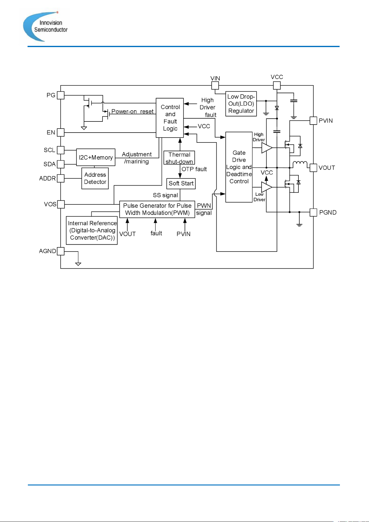
7
Innovision Semiconductor
Preliminary Datasheet
ISM6636A/B
Rev1.10 01/2023
Electrical Characteristics
Unless otherwise stated, specifications apply over: 5V < PVIN = VIN< 16V, 0°C < TA <
125°C,Typical values are specified at TA= 25°C
PARAMETER
CONDITIONS
MIN
TYP
MAX
UNIT
Supply Current
I
IN
(STANDBY)
VIN Supply Current
(Standby)
Enable low
1
mA
I
IN
(STATIC)
VIN Supply Current
(Static)
No switching, EN = 2V
2.3
I
IN
(DYN)
VIN Supply Current
(Dynamic)
EN high, VIN = 12V, V
OUT
= 5.0V, F
SW
=
1.875MHz(Note 2)
23
Soft-Start
SS
VOS Soft-Start Rate
Default
1
V/ms
Output Voltage
VOUT
VOUT (default)
5
V
Resolution
10
mV
Accuracy
Tj= 25°C, PVIN = 12V,
VOUT = 5V
±0.5
%
25°C< Tj< 125°C, PVIN =
12V, VOUT= 3.3V
-1
1
25°C< Tj< 125°C, PVIN =
12V, VOUT= 5V
-1.2
1.2
On-Time Timer Control
T
ON
On Time
PVIN = 12V, VOUT = 5V,
FSW = 1.875MHz
222
ns
T
ON
(MIN)
Minimum On-Time
(Note 2)
40
T
OFF
(MIN)
Minimum Off-Time
(Note 2)
184
SW Frequency
Fsw
SW Frequency
PVIN = 12V, VOUT =
3.3V, VOS connect to
VOUT.
1.875
MHz
PVIN = 12V, VOUT =
5.0V, VOS connect to
VOUT.
1.875
Accuracy
-15
+15
%
Internal Low Drop-Out (LDO) Regulator
VCC
LDO Regulator
Output Voltage
5.5V < VIN ≤ 16V, 0 -
20mA
4.8
5
5.2
V
5 ≤ VIN< 5.5V, 0 - 20mA
4.3
VLN
Line Regulation
5.5V < VIN ≤ 16V, 20mA
200
mV
VLD
Load Regulation
VIN = 12V, 0 - 20mA
100
8
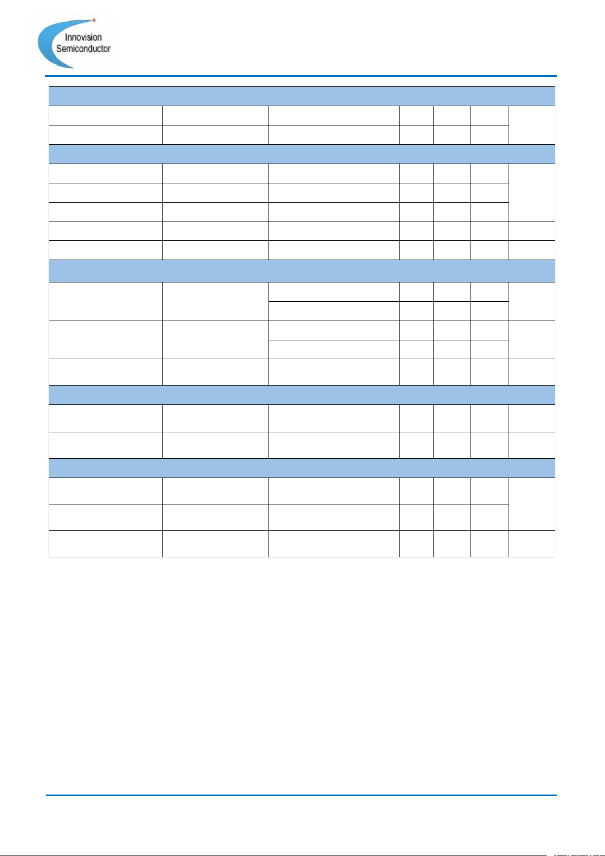
Innovision Semiconductor
Preliminary Datasheet
ISM6636A/B
Rev1.10 01/2023
Thermal Shut-Down
TSD (default)
Thermal Shut-Down
145
°C
Hysteresis
25
Under-Voltage Lock-Out and Enable
VCC_UVLO(START)
VCC Start Threshold
VCC Rising Trip Level
3.7
4.0
4.2
V
VCC_UVLO(STOP)
VCC Stop Threshold
VCC Falling Trip Level
3.6
3.8
3.95
En(HIGH)
Enable Threshold
Ramping Up
1.1
1.2
1.3
En(LOW)
Enable Threshold
Ramping Down
0.95
1
1.05
V
REN
Input Impedance
3V < V
EN
< 18V
500
1000
1500
kΩ
Current Limit
IOC
DC IOUT Current
limit
TJ = 25°C, VOUT = 3.3V,
5
5.7
6.4
A
TJ = 25°C, VOUT = 5V,
4.7
5.4
6.1
Val_OC
Valley Current Limit
TJ = 25°C, VOUT = 3.3V
3.8
4.3
4.8
A
TJ = 25°C, VOUT = 5V
3.8
4.3
4.8
TBLK(HICCUP)
Hiccup Blanking
Time
(Note 2)
25
ms
Over-Voltage Protection
VOVP
Output Over-Voltage
Protection Threshold
OVP Detect
OV_Threshold[1:0] = 11
115
120
125
VOS%
TOVPDEL
Output Over-voltage
Protection Delay
(Note 2)
7
µs
Power Good (PG)
VPG(UPPER)(default)
Power Good Upper
Threshold
VOUT Rising
85
90
95
VOS%
VPG(LOWER)
Power Good
Hysteresis
VOUT Falling
5
IPG
Power Good Sink
Current
PG = 0.5V, En = 2V
10
mA