Specification_SIPLACE_S23HM_eng.pdf - 第19页
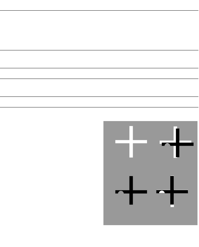
18 Description Different reference mark shapes prove to be optimal depending on the condition of the surface. Particul arly advi sable for bare co p- per su rfaces with little oxida tion is the single cross. Maximum reco…
17
Target Low
Structure Correlation
Description
With the SIPLACE S-23 HM, sev-
eral vision modules with a central
vision system to analyze recorded
image data ensure high placement
precision.
At one of the machine’s two X-
gantries the PCB vision module
recognizes offsets in the position
of the PCB in the conveyor sys-
tem. The modules are also re-
quired to scan the machine or the
feeders on one side of the table.
Each vision module consists of a
CCD camera with integrated light-
ing and optics.
The offsets in PCB position are de-
termined with the help of at least
two - but generally three - refer-
ence marks on the PCB. When the
PCB arrives, the gantry with its
PCB vision module moves to the
programmed mark position. The
vision system compares the re-
corded video image with the sam-
ple stored in the PCB description.
By applying the correlation princi-
ple the vision system can deter-
mine the correct position through
comparisons with programmed
target structures even when refer-
ence marks are incomplete or
damaged (actual structures).
The shapes are not inviolably
specified; they can be taught with-
out restrictions.
Additional functions of the PCB vi-
sion module are the position rec-
ognition of the feeders and ce-
ramic substrates (optional) and the
calculation of processing data in-
cluding mapping.
In addition, recognition of faulty
PCBs is conducted via ”ink spots”
with the aid of the PCB vision
module.
Vision Sensor Technology:
PCB Vision Module
Technical Data
Reference marks
Local marks
Library memory
Recognition of poor panels
up to 3 (subpanels and multiple panels)
up to 2 per component
(may be of different type)
up to 255 types of reference marks
per subpanel
Image analysis Correlation principle
based on gray-scale values
Lighting method Front lighting
Recognition time
mark/ink spot
0.8 s
Camera’s field of view 5.7 x 5.7 mm
Correlation Principle
Actual High
Structure Correlation
18
Description
Different reference mark shapes
prove to be optimal depending on
the condition of the surface.
Particularly advisable for bare cop-
per surfaces with little oxidation is
the single cross. Maximum recog-
nition reliability is achieved due to
the high information content. Rec-
tangle, square and circle are less
”informative” but save space, are
rugged, and can even be used
when oxidation is at an advanced
stage.
Advisable for tinned structures are
circle or square because in this
case the ratio of the mark dimen-
sions to the presolder thickness is
particularly favorable.
Vision Sensor Technology:
PCB Position Recognition
Template
Window
PCB Camera
Field of View
Search
Area
Fiducial to
Be Located
Reference
Fiducal
Reference Mark Criteria
Locate 2 marks
Locate 3 marks in addition
X-/Y-position, rotation angle, mean dis-
tortion
Shear, distortion in X- and Y-direction
Mark shapes Freely definable via teaching, e.g.,
single cross, rectangle, square, circle
Mark surface
Copper
Tin
Without oxidation and solder resist
Warp ≤ 1/10 of structure width,
good contrast to environment
Mark dimensions
single cross
rectangle/square
circle
Length and width: 0.9 - 2 mm
Line thickness: 0.3 - 1.0 mm
Edge length: 0.5 - 2 mm
Diameter: 0.5 - 2 mm
Mark environment Clearance around reference mark not
necessary if there is no similar mark
structure in the search area
(5.7 x 5.7 mm)

19
Description
In cluster technology, each sub-
panel is assigned an ink spot. If
this is present when the PCB vi-
sion module conducts the meas-
urement, the pertinent subpanel is
not populated.
Naturally, it is also possible to pre-
vent the population of the sub-
panel when the ink spot is miss-
ing.
This function can be used to pre-
vent costs incurred by unneces-
sarily populating faulty subpanels.
P
PP
Po
oo
os
ss
si
ii
it
tt
ti
ii
io
oo
on
n n
n R
RR
Re
ee
ec
cc
co
oo
og
gg
gn
nn
ni
ii
it
tt
ti
ii
io
oo
on
n n
n o
oo
of
f f
f F
FF
Fee
eeee
eed
dd
de
ee
er
rr
r
The pick-up position of the com-
ponents can be determined pre-
cisely with the aid of the position
recognition of the feeder. It is acti-
vated each time after a change of
feeder or component table. The
offset in position relative to the
stored ideal position is determined
on the basis of fiducials on the
feeder modules using the PCB vi-
sion module. This provides a very
high pick-up reliability even for the
very first component. This is par-
ticularly important with small com-
ponents.
Vision Sensor Technology:
Recognition of Faulty PCBs via Ink Spots
Position Recognition of Feeder
Ink Spot Criteria
Mark shapes Single cross (recommended because
of lowest susceptibility to problems),
rectangle, square, circle, etc.
Masking material Mat dark (light-absorbent)
Not advisable: white or glossy
Size of mark masking
Circular: Diameter ≥ 8.1 mm
Square: Edge length ≥ 5.7 mm
Mark recognition time
(Travel > 100 mm)
Mark masked: 1.2 s
Mark not masked: 0.4 s