X service技术参数 - 第37页
37 Vision Sensor Technology Bad Board Recognition Position Recognitio n for Feeder Modu les Ink Spot Criter ia Evaluation met hod for f id uc ia ls for structures brightness m ethod contrast me thod Shap es an d si zes o…
36
Vision Sensor Technology
PCB Position Recognition
Fiducial criteria
Locate 2 fiducials
Locate 3 fiducials
X-/Y-position, rotation angle,
mean PCB distortion
in addition: shear, distortion in X- and
Y-direction separately
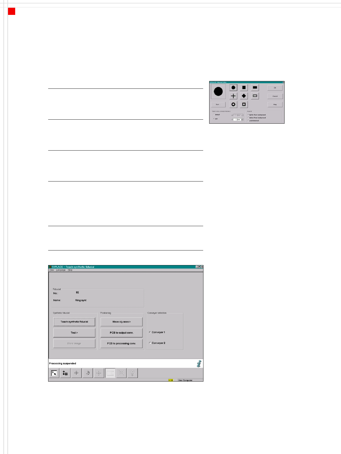
Fiducial shapes Choose synthetic fiducials from the
menu: circle, cross, square, rectangle,
rhombus, circular, square, and rectan-
gular contours
Fiducial surface:
Copper
Tin
Without oxidation and solder resist
Warp ≤ 1/10 of structure width, both
with good contrast to environment
Fiducial dimensions:
Circle
Cross
Rectangle/square
Rhombus
Diameter: 0.3 - 3 mm
Length and width: 0.3 - 3 mm
Line thickness: 0.1 - 1.5 mm
Edge length: 0.3 - 3 mm
Diagonal: 0.3 - 3 mm
Fiducial environ-
ment
Clearance around reference fiducial
not necessary if there is no similar
fiducial structure in the search area
Teach Synthetic Fiducial
Description
Different fiducial shapes
prove to be optimal depend-
ing on the condition of the
surface.
Particularly advisable for bare
copper surfaces with little
oxidation is the single cross.
Maximum recognition reli-
ability is achieved due to the
high information content.
Rectangle, square and circle
are less “informative” but
save space, are rugged, and
can even be used when oxi-
dation is at an advanced
stage.
Advisable for tinned struc-
tures are circle or square
because in this case the ratio
of the fiducial dimensions to
the presolder thickness is
particularly favorable.
Fiducial editor

37
Vision Sensor Technology
Bad Board Recognition
Position Recognition for Feeder Modules
Ink Spot Criteria
Evaluation method
for fiducials
for structures
brightness method
contrast method
Shapes and sizes of fidu-
cials/structures for
brightness method
contrast method
square or circular forms
edge length / diameter 0.3
to 5 mm
rectangular shapes
edge length: 0.3 to 5 mm
Masking material mat dark (light-absorbing)
not recommended: white or
shiny
Recognition time 0.3 s for each method
Description
In the cluster technology
each subpanel is assigned an
ink spot. If this is present dur-
ing the measurement via the
PCB vision module, the corre-
sponding subpanel is popu-
lated.
It is also possible to accom-
plish the population of the
subpanel when the ink spot is
missing. With this function it
is possible to eliminate costs
due to unnecessary popula-
tion of faulty subpanels.
Global Ink Spot
Each GOOD/SCRAP scan takes
some time, and the time
required is even greater if
there are a large number of
subpanels on a PCB. Using
the global ink spot can result
in a significant reduction of
these secondary times.
The PCB vision module
searches at positions taught
before for the defined fidu-
cial. In case of recognition
there is no following evalua-
tion of subpanels. The sys-
tem allows the operator to
choose also the reverse inter-
pretation.
Recognition of the position
of the feeder modules
The pick-up position of the
components can be deter-
mined precisely with the aid
of the position recognition
for the feeder. The offset in
position relative to the stored
ideal position is determined
on the basis of fiducials on
the feeder modules using the
PCB vision module. This pro-
vides a very high pick-up reli-
ability even for the very first
component. This is particu-
larly important for small com-
ponents.

38
Technical Data
Siemens Signal Interface
Connector Assignment
Signal interface (20-pin ribbon cable connector)
Upstream station X1 Downstream station X2
Pin 1 Reserved Pin 1 Reserved
Pin 2 GND 24 VDC Pin 2 Reserved
Pin 3 + 24 VDC Pin 3 Reserved
Pin 4 Reserved Pin 4 Reserved
Pin 5 Reserved Pin 5 GND 24 VDC
Pin 6 Reserved Pin 6 + 24 VDC
Pin 7 Reserved Pin 7 Reserved
Pin 8 Reserved Pin 8 Reserved
Pin 9 Reserved Pin 9 Reserved
Pin 10 Reserved Pin 10 Reserved
Pin 11 Interfering signal loop Pin 11 Interfering signal loop
Pin 12 Interfering signal loop Pin 12 Interfering signal loop
Pin 13 GND 24 VDC Pin 13 GND 24 VDC for permission /
arrived (galvanic isolation)
Pin 14 Arrived Pin 14 Arrived
Pin 15 Permission Pin 15 Permission
Pin 16 Reserved Pin 16 Reserved
Pin 17 Reserved Pin 17 Reserved
Pin 18 Transferred Pin 18 Transferred
Pin 19 Request Pin 19 Request
Pin 20 GND 24 VDC for request / trans-
ferred (galvanic isolation)
Pin 20 GND 24 VDC