Detailed Circuit Diagram Folder SIPLACE F5.pdf - 第107页
4 Printed Circui t Boards 107 I 0032118 9-030 101ND4 820 P C boar d, conversion bo ard, lar ge axis ( Sh. 1 of 2) 0032118 9-030 101ND4 820 P C boar d, conversion bo ard, lar ge axis ( Sh. 2 of 2) Stat. 03 04 Modified 09.…
4 Printed Circuit Boards 106
I
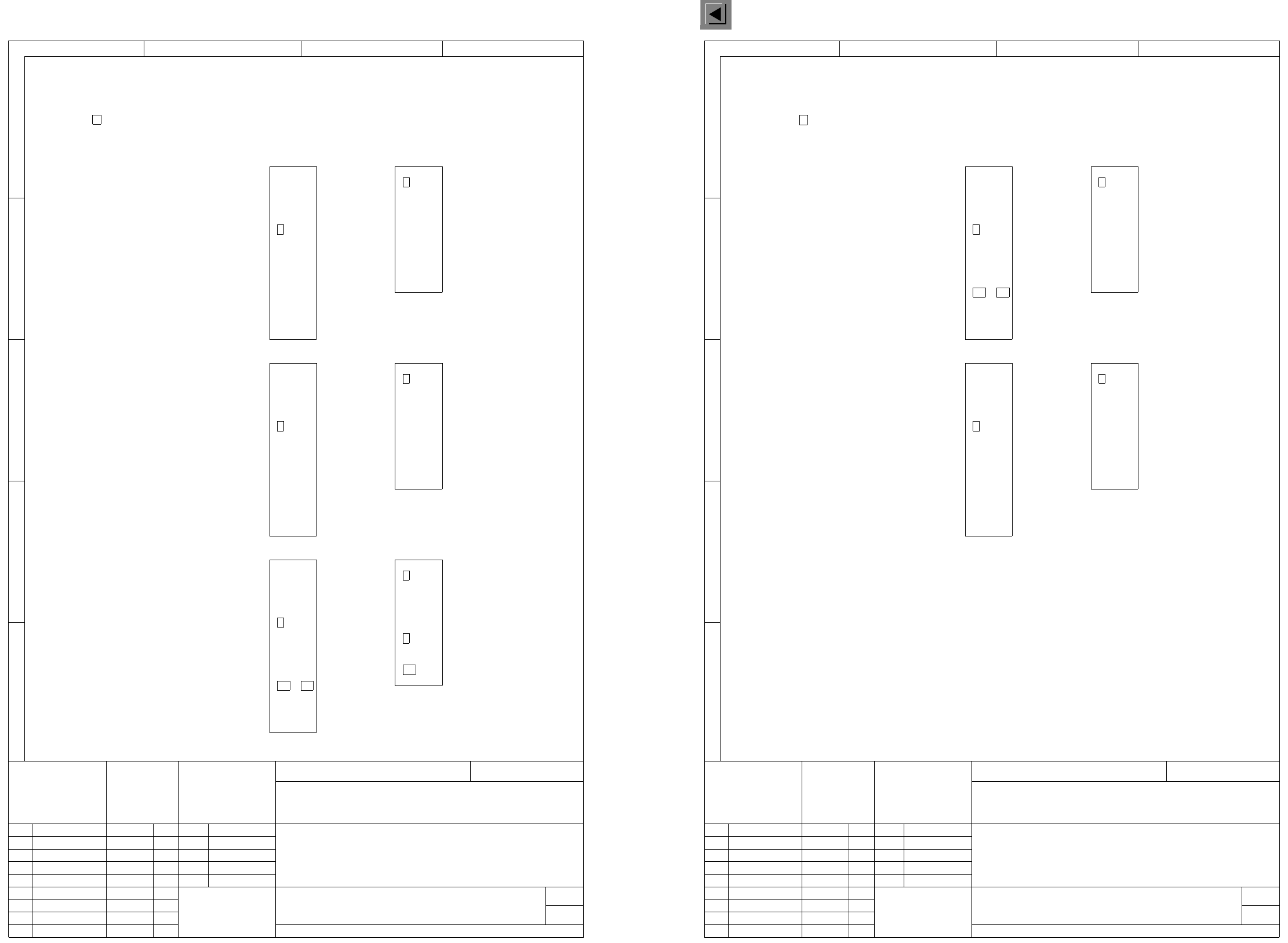
00321036-010101FD4 Axis rear panel I (axis 166)
00321037-010101FD4 Axis rear panel II (axis 166)
14
7
X6X5Star axis
7
2019
1817
16
1413
1211
10
8
65
43
9
21
7
2019
1817
1615
1413
1211
10
8
65
43
9
21
7
2019
1817
1615
1413
1211
10
8
65
43
9
21
15
321036-01
Siemens AG
AUT5-BSM
4321
E
D
C
B
A
XX
XXXX
X
X
X
X
X
X
X
Product status
Doc. status
1
1
SMD Placement System Siplace 80S20
Stat. Modified Date Name
Date
Author
Check.
Stand.
Sh.
Sh.
Scale
Mat. no.:
18.07.1995
Sz
00321036-010101FD4
Axis rear panel I
(axis 166)
1:1
1.
1. Sz
Sz
18.07.95
18.07.95
Remove all key pins marked with
an X from the axis rear panel.
12
9
34
56
8
10
11 12
13 14
7
X2X1X axis
12
9
34
56
8
10
11 12
13 14
7
X4X3Y axis
12
9
34
56
8
10
11 12
13
10
8
65
43
9
21
7
2019
1817
16
1413
1211
10
8
65
43
9
21
15
321037-01
XXXX
X
X
X
X
Siemens AG
AUT5-BSM
4321
E
D
C
B
A
Product status
Doc. status
1
1
SMD Placement System Siplace 80S20
Stat. Modified Date Name
Date
Author
Check.
Stand.
Scale
Sh.
Sh.
Mat. no.:
18.07.1995
Sz
00321037-010101FD4
Axis rear panel II
(axis 166)
1:1
1.
1. Sz
Sz
18.07.95
18.07.95
Remove all key pins marked with
an X from the axis rear panel.
12
9
34
56
8
10
11 12
13 14
7
X2X1Z-SP axis
12
9
34
56
8
10
11 12
13 14
7
X4X3Rotate SP axis
7
2019
1817
1615
1413
1211
4 Printed Circuit Boards 107
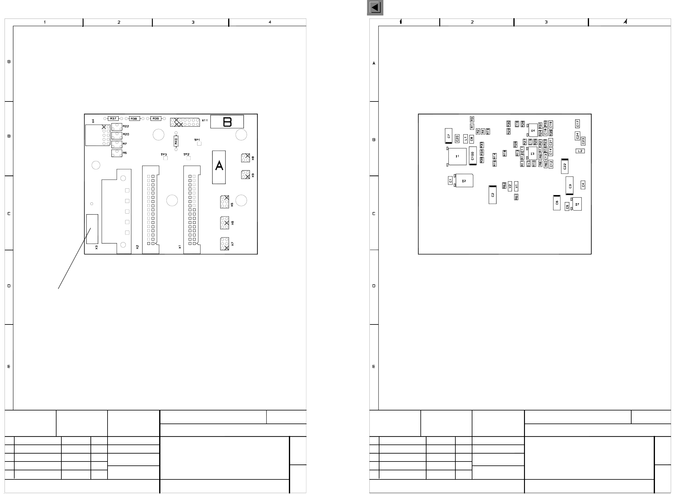
I
00321189-030101ND4 820 PC board, conversion board, large axis (Sh. 1 of 2)
00321189-030101ND4 820 PC board, conversion board, large axis (Sh. 2 of 2)
Stat.
03
04
Modified
09.10.97
27.03.97
Date
KD
KD
Name
PC board
Dorfner
12.02.97
FSZ MCHN
SIEMENS AG
TD E E
Date
Name
4-layer
G32918 - J2 - B001 - * - 17
Conversion board, large axis
00321189-030101ND4
PC board
Scale
1 : 1
820
1 +
Sheet
Component mounting diagram, component side
Document identification
Remove all pins marked with an X
A = identification label
B = inspection label
03
Stat.
04
Modified Date
27.03.97
09.10.97
Name
KD
KD
TD E E
SIEMENS AG
FSZ MCHN
12.02.97
Dorfner
PC board
Date
Name
00321189-030101ND4
Conversion board, large axis
G32918 - J2 - B001 - * - 17
PC board
Scale
1 : 1
820
Component mounting diagram, solder side
Sheet
2 -
4 Printed Circuit Boards 108
I
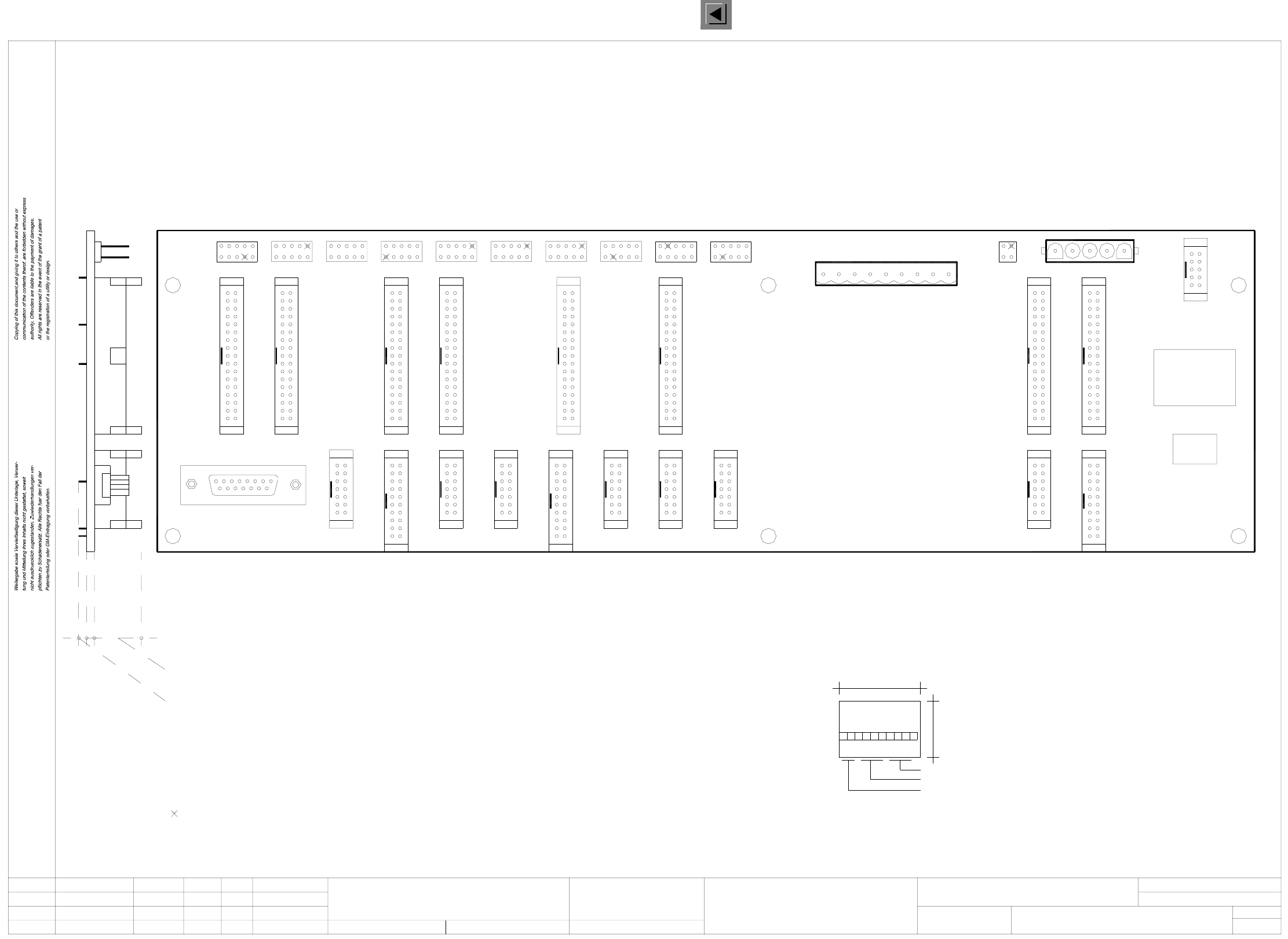
00321190-030101ND3 Gantry conversion board
29.08.2000
Haas
Conversion board
gantry
01. Haas
03. Haas
00321190
SIEMENS AUT 5
25
Numerals
Date (year/month/day) according to SN 01007
Manufacturer/location of plant according to SN 37040
AA-BBBB-CCCC
P123456789
PCB thickness = 1.7 mm
(except for the plug X12, X13 = 2.5 mm)
The following labels have to be applied:
A: Identification label, assembly inscription acc. to VA-F-510-001
Maximum leads height on bottom = 1 mm
(plug with locking lever)
Maximum component height on top = 19 mm
X14
1
X121
X24X25X26X27X28X29X30X31X32X33
1
X10
X34
1
1
X11
X22
1
1
X23
X8
1
1
X4
1
X3
1
X2
1
X1
1
X16
1
X17
1
1
X19
1
X20
1
X21
1
X13
X36X35
X15
X18
1
1
1
40
B: Inspection label
X7
1
11
1111111
1
Pinch off this pin
Haas01.
00321190-030101ND3
*)
29.08.2000
29.08.2000
29.08.2000
Stromlaufplan/Circuit diagram
1816151413121110987654321 17
Function status
Product status
Doc. status
SMD Placement System Siplace 80S
1
1Status Modified Date Name Stand.
Check.
Author
Date
Orig. Ers.f. Ers.d.
Sh.
Sh.
PLEA1 E
SIEMENS AG
*) Insert dummy plug in
post plug X8
A
B