Detailed Circuit Diagram Folder SIPLACE F5.pdf - 第110页
4 Printed Circui t Boards 110 I 0032133 6-010 101FD4 A xis rear panel I II (axis 1 66) 18.0 7.199 5 Sz 003213 36- 010101 FD4 Axi s rea r panel II I (axi s 166) 1:1 1. 1. Sz Sz 18.07.9 5 18.07.9 5 Rem ove a ll key pins ma…
4 Printed Circuit Boards 109
I
00321213-040101ND4 Adjustment unit, SP6_12 placement head
SIEMENS AG
1.
1.
4.
F
1
Doc. status
Product status
Function status
E
D
23
19.06.97
PL EA1 E2
4
C
B
A
1234
SMD Placement System SIPLACE HS50
00321213-040101ND4
5
Adjustment unit
678
1
+
=
Sheet
Sh.
1
F
E
D
567
C
B
8
A
SP6_12 placement head
R2
R2R2
R2 R2
V2
V1
X2
X3
h1
h2
Status Modified Date Name
Date
Author
Check.
Stand. Orig. Creat. f. Creat. by
4 Printed Circuit Boards 110
I
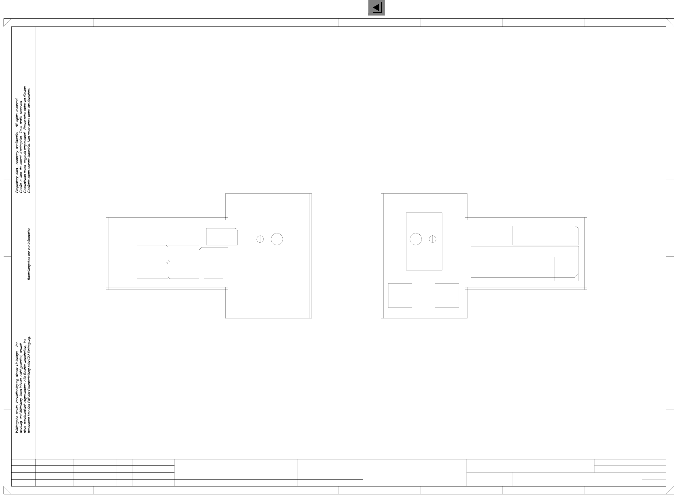
00321336-010101FD4 Axis rear panel III (axis 166)
18.07.1995
Sz
00321336-010101FD4
Axis rear panel III
(axis 166)
1:1
1.
1. Sz
Sz
18.07.95
18.07.95
Remove all key pins marked with X
from the axis rear panel.
12
9
34
56
8
10
11 12
13 14
7
X2X1
Z-IC axis
12
9
34
56
8
10
11 12
13 14
7
X4X3Rotate IC axis
7
2019
1817
1615
1413
1211
10
8
65
43
9
21
7
2019
1817
16
1413
1211
10
8
65
43
9
21
15
321336-01
XXXX
XXXX
X
X
X
X
Siemens AG
AUT5-BSM
4321
E
D
C
B
A
SMD Placement System Siplace 80
Doc. status
1
1
Product status
Stat. Modified Date Name
Date
Author
Check.
Stand.
Scale
Sh.
Sh.
Mat. no.:
4 Printed Circuit Boards 111
I
00321469-040101ND3 Component illumination
Siemens AG
AUT5-BSM
MS-Elektronik
01.
04.
25.11.98
Document. status
Hi
25.11.98
Function status
1
Dorn
2 6
25.11.98
345 789
00321469-040101ND3
Components illumination
Stromlaufplan/Circuit diagram
10 11 12
SIPLACE HS50
13 14 15
Sh.
1716 18
Sh.1
1
19
R52
V3
V12
R15
Maximum component height: ON TOP 10.0 mm, ON BOTTOM 14.0 mm
R56
V11
V18
V9
R39
V10
R13
R31
R21
R30
R50
J6
C13
C9
R37
R28
R10
R19
R18
V22
R48
R3
R47
R42
V14 V13V17 V16 V15
V6
R27
V7V8
R12
R38
R29
R11
R20
R4
R22
C8
J2
J1
J3
V23
R54
C10
R45
R44
J4
V24
R41
R40
R32
R53
V19
R2
R57
R1
R58
R5
V2
X4 X1
Remove all pins marked with an x.
The following labels have to be stuck on!
C1 to C3 have to be glued!
A: Identification label
B: Inspection label
C: ESD label
V1
R55
V21
R43
R33
R24
R6
R14
V4V5
R35
R26
R36
R9
R17
R49
R46
R51
V20
P2
P3
X3
X2
C2
C3
C1
R34
R25
R8
R7
R16
P1
Product status
01.
25.11.98
Status Modified Date Name Stand.
Check.
Author
Date
Orig./Creat. f./Creat.by
R23
C12
C11
J5
C5
C4
C6
C7