Detailed Circuit Diagram Folder SIPLACE F5.pdf - 第122页
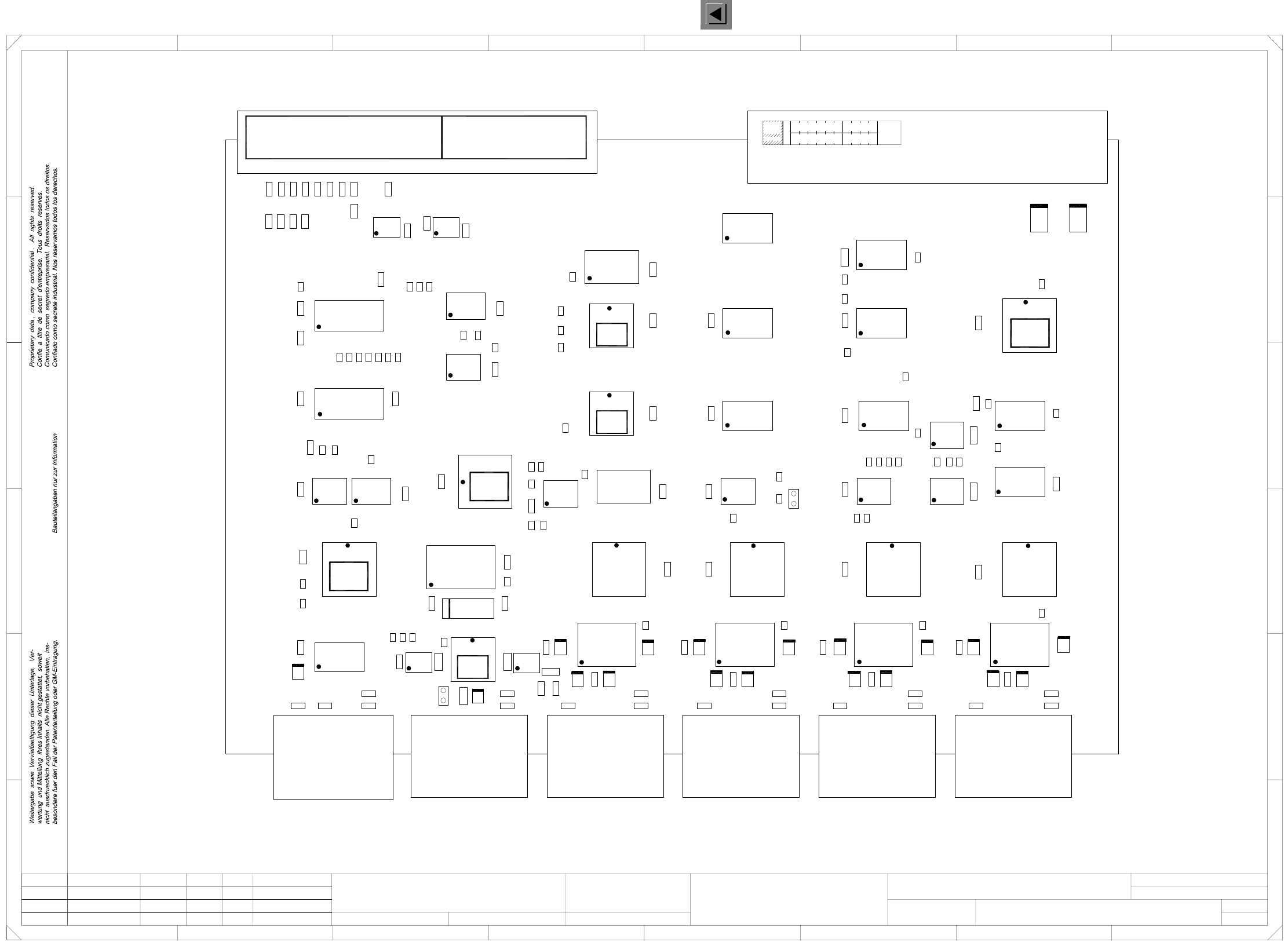
4 Printed Circui t Boards 122 I 0032614 2-050 101ND3 KSP-COM 351 co mmunicatio ns assem bly C51 C52 C53 C54 C55 C56 C58 C59 C6 C60 C61 C62 C63 C7 C8 C81 C82 C83 C84 C86 C87 C9 C90 C91 C92 C93 C94 C95 C96 C97 C98 C99 C24 …
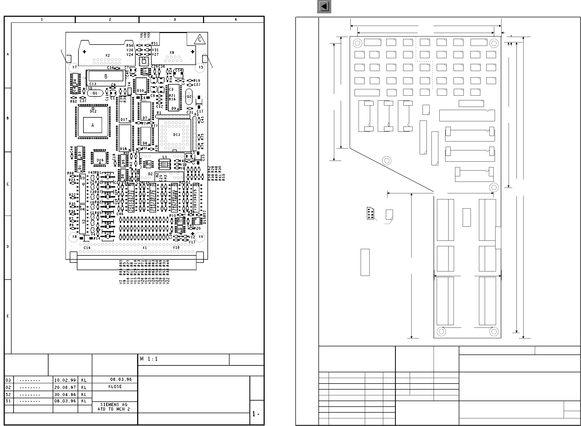
4 Printed Circuit Boards 121
I
00325579-020101ND4 776 PC board, step motor control, control unit
00325581-030101MD4 Conversion board, PCB conveyor
Technische Dokumentation Hick, Technische Dokumentation Hick 18.05.00 10:10 00325579-020101ND4_ST.dwg
A = IDENTIFICATION LABEL ON THE BACK
B = INSPECTION LABEL ON THE BACK
C = ESD LABEL ON THE BACK
PCB 776
STEP MOTOR CONTROL
CONTROL UNIT
COMPONENT MOUNTING DIAGRAM
6-LAYER PCB
G32918-H0007-B001-*-17
00325579-020101ND4
Sheet
Stat. Modified Date Name
Date
Name
1.
3.
1.
10.04.97
10.04.97
10.04.97 Tu.
Tu.
Tu.
02.07.1996
02.07.1996
00325581-030101MD4
s
Aktiengesellschaft
AUT 5 EBS 8
Datum
Bearb.
Gepr.
Norm
Name
Dateiname:
Zust.
Mitteilung Datum
Name
(Materialnummer)
Format A4
Mat.-Nr.: FS ES US S/F
Blatt
Maßstab
Weitergabe sowie Vervielfältigung dieser Unterlage, Verwertung und Mitteilung
ihres Inhaltes nicht gestattet, soweit nicht ausdrücklich zugestanden.
Zuwiderhandlungen verpflichten zu Schadenersatz. Alle Rechte für den Fall
der Patenterteilung oder GM-Eintragung vorbehalten.
Copying of this document, and giving it to others and the use or communication
of the contents thereof, are forbidden without express authority. Offenders are
liable to the payment of damages. All rights are reserved in the event of the
grant of a patent or the registration of the utility model or design.
X12 20 pol AMP
X13 20pol AMP
270 mm
130 mm
135mm
100 mm
60 mm
48mm
258 mm
129 mm
6 mm
6 mm123 mm
104 mm
94 mm
Pin 1
Key 1
Key 1
Key 1
Key 2
Key 2
Key 2
X45
5
X16
10
5
X24
5
X22
X20
1
X18
3
X42
5
X30
1
X48
4
X44
X38
1
X32
4
X26 X28
5
X36
4
X34
1
X40
4
X46
4
X6
BK-Mod 30pol
X8
BK-Mod 26pol
X10
BK-Mod 26pol
X7
BK-Mod 20pol
X5
BK-Mod 14pol
X3
BK-Mod 14pol
X4
BK-Mod 14pol
J1
X47 X45
5
X41 X43
4
X19
3
X21
1
X23
X49
5
X35
1
X37
4
X39
1
X33
1
X27
X31
4
X29
1
X17
9
25
5
X2
Combicon 7pol.
.1
X1
Combicon 7pol
1.
X14
Combi. 4pol
.1
X15
Combi. 4pol
1.
X11
Combicon 8pol
1.
X9
Combicon 8pol.
.1
00325581.M31
1/1
Siemens AUT 5
00325581-01
B
A
X57
2 und 13
X56
1 + 14
X55
5
X53
1
X51
4
X50
1
X52
5
X54
1
14
15
Siplace 80S20/F4 SMD placement system
Conversion board, PCB conveyor
Function status
Product status
Document. status
6 Bohrungen D=4,5 mm
Toleranzen +/- 0,1mm
Plugs X12, X13, X16 - X49
viewed from top
Plug designation
and coding (pin no.)
Combicon plug coding
Codierreiter CR-MSTB Item no.: 1734401
J1 Jumper on pins 1-2
A Inscription label
B Inspection label
4 Printed Circuit Boards 122
I
00326142-050101ND3 KSP-COM351 communications assembly
C51
C52
C53
C54
C55
C56
C58
C59
C6
C60C61
C62
C63
C7
C8
C81
C82
C83
C84
C86
C87
C9
C90
C91
C92
C93
C94
C95
C96
C97
C98
C99
C24
C25
C26
C27
C28
C29
C30
C31
C32
C33
C34
C35
C46
C47
C48
C49
C89
C36
C37
C88
D1
D16
D17
D18
D2
D3
D4
D45
R37
R38
R39
R4
R40
R41
R42
R43
R44
R45
R46
R47
R48
R49
R5
R50
R51
R52
R53
R55
R56
R57
R58
R59
R6
R60
R61
R62
R63
R66
R67
R69
R7
R10
R65
R20
R21
R64
R54
R68
R70
R71
R72
R73
R9
X1
X10
X9
X2X3X4X5
X6
X7
X8
D46
D10
D11
D19
D38
D5
D8D9
D12
D13
D14
D15
D20
D21
D31
D32
D49
D22
D40
D41
D47
D48
D6
D7
D23
D27
D50
D25
D43
D29
D35
G1
G2
G3
R1
R11
R12
R13
R15
R16
R17
R18
R19
R2
R22
R23
R24
R25
R26
R27
R28
R29
R3
R30
R31
R32
R33
R34
R35
R36
C1
C118
C119
C120
C121
C10
C100
C101
C102
C103
C104
C105
C106
C107
C108
C109
C11
C110
C111
C112
C113
C114
C115
C116
C117
C12
C13
C14
C15
C16
C17
C18
C19
C2
C20
C21
C22
C23
C3
C4
C42
C43
C44
C45
C5
C50
200031810
D5 V1.0
PCA82C200T
Right angle male
D-SUB, 9-pole
Right angle female
D-SUB, 9-pole
Right angle male
D-SUB, 9-pole
Right angle male
D-SUB, 9-pole
Right angle male
D-SUB, 9-pole
Right angle male
D-SUB, 9-pole
Male multipoint connector, 64-pole
Male multipoint connector, 96-pole
6A
7
TESTED
LB
98
1
O
4
98
23
DN
5
M4
60
L
M
SH
I
V
R
multipoint connectormultipoint connector Stiftleiste 9-polemultipoint connectormultipoint connectormultipoint connector
Status Modified Date Name Stand.
Date
Check.
Orig. Creat. f. Creat. by
Author
MADE IN GERMANY
SIEMENS
KSP-COM351 LB XXXXXX
6AR1313-0FA03-0AA0 KS:XX
TZ AUT5 00326142-XX
47p
47p
47p
47p
NB
NB
NB
NB
120
120
120
120
100n
100n
100n
100n
47p
47p
100
120
1k
100
10k
10k
10k
75179
75179
IDT7202
74HCT151
IDT7202
74HCT02
10k
10k
10k
10k
10k
10k
10k
1k
1k
1k
1k
1k
1k
1k
1k
1k
10k
100n
100n
47p
47p
74HCT164
74HCT174
74HCT74
N82510
oder
SJA1000T
GAL20V8
200031810
D19 V2.0
GAL26VC12
200031810
D38 V1.0
100n
100n
100n
100n
100n
100n
1k
1k
1k
10k
10k
10k
10k
10k
10k
10k
10k
GAL16V8
200031810
D50 V1.0
74HCT244
MA-505
16.00 MHz
PCA
82C250T
PCA
82C250T
100n
100n
100n
100n
100n
100n
22p
22p
47p
47p
47p
3n3
47p
47p
47p
47p 47p
1u/
35V
1u/
35V
1u/
35V
1u/
35V
0
NB
NB
120
120
1k
SG615
74HCT245
74HCT245
74HCT245
20MHz
100n
100n
100n
100n
100n
GAL18V10
200031810
D27 V1.0
GAL16V8
200031810
D23 V1.0
18,432MHz
SG615
74HCT04
N82510
MAX209
MAX209
1u/
35V
1u/
35V
1u/
35V
100n
100n
100n
100n
100n
10k
1k
1k
1k
10k
1u/
35V
1u/
35V
1u/
35V
47p
47p
47p
47p
47p
100n
74HCT245
74HCT245
100n
100n
100n
10u/
25V
10u/
25V
1k 1k
1k
1k
10k
1k
0
0
0
0
47k
1k
1k
1k
1k
1k
1k
1k
1k
100n
100n
100n
100n
100n
100n
74HCT245
74HCT273
74HCT573
74HCT86
74HCT86
74LS06
N82510 N82510
MAX209
MAX209
100n
100n
100n
100n
1k
1k
1u/
35V
1u/
35V
1u/
35V
1u/
35V
1u/
35V
1u/
35V
1u/
35V
1u/
35V
47p
47p
47p
47p
47p
47p
100n
100n
GAL26VC12
A
1234
SMD Placement System SIPLACE HS50
00326142-050101ND3
5
Communication assembly
678
1
+
=
Sheet
Sh.
1
F
E
D
567
C
B
8
A
KSP-COM351
SIEMENS AG
Seer
1.
1.
1.
F
1
Doc. status
Product status
Function status
Seer
Seer
Seer
12.10.98
12.10.98
12.10.98
E
D
23
12.10.1998
PL EA1 E2
4
C
B
4 Printed Circuit Boards 123
I
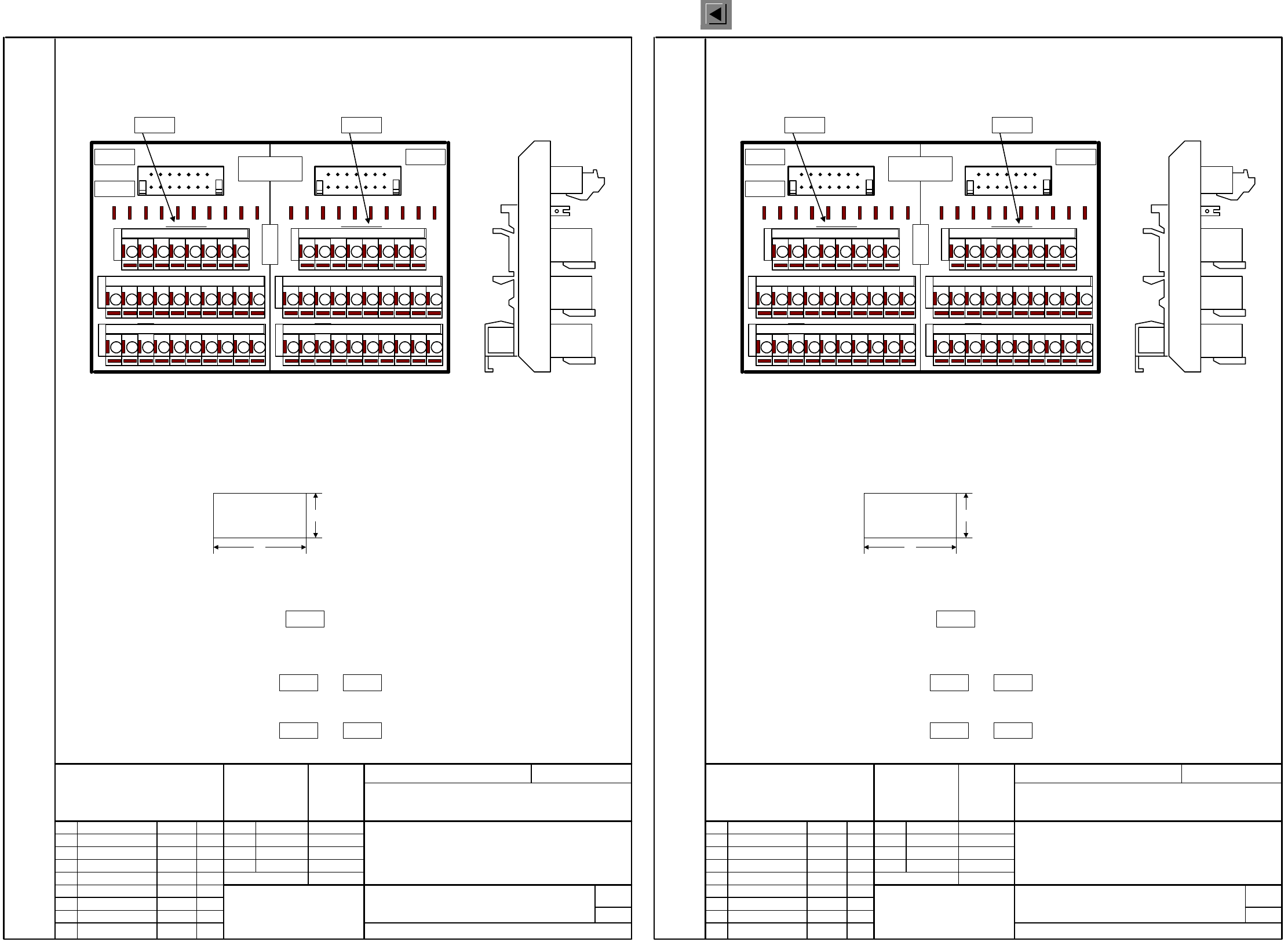
00327250-010101MD4 I/O terminal board A1
00327251-010101MD4 I/O terminal board A2
1.
1.
1.
11.06.96
11.06.96
11.06.96 Tu.
Tu.
Tu.
11.06.1996
11.06.1996
00327250-010101MD4
SIEMENS
Aktiengesellschaft
AUT 5 BPB BS1
Datum
Bearb.
Gepr.
Norm
Name
Dateiname:
Zust.
Mitteilung
Datum
Name
(Materialnummer)
Format A4
Mat.-Nr.: FS ES US S/F
Blatt
Maßstab
Weitergabe sowie Vervielfältigung dieser Unterlage, Verwertung und Mitteilung
ihres Inhaltes nicht gestattet, soweit nicht ausdrücklich zugestanden.
Zuwiderhandlungen verpflichten zu Schadenersatz. Alle Rechte für den Fall
der Patenterteilung oder GM-Eintragung vorbehalten.
Copying of this document, and giving it to others and the use or communication
of the contents thereof, are forbidden without express authority. Offenders are
liable to the payment of damages. All rights are reserved in the event of the
grant of a patent or the registration of the utility model or design.
(a1_1zu1.vsd)
00327250.11M
M -
-
- - - - -- M
P +
+
+ + + + ++ P
2
3
4 5 6 7 81
M -
-
- - - - -- M
P +
+
+ + + + ++ P
2
3
4 5 6 7 81
A
X2kb
B
X1ka
1/1
X1ka
A1
X2ka
Siemens AUT5
00327250-01
AA-BBBB-CCCC
15
10
X1kb
X2kb
X2ka
X1kb
1 2 3 4 5 6 7 8
P + + + + + + + + P
M - - - - - - - - M
1 2 3 4 5 6 7 8
P + + + + + + + + P
M - - - - - - - - M
A1
Function status
Document status
Product status
SMD Placement System Siplace
I/O terminal board A1
The following labels have to be stuck on:
1 : Assembly designation
Attach the terminal designation to the terminals.
2 : Plug designation
A : Identification label
B : Inspection label
Assembly inscription acc. to recommendation VA-F-510-001
font size 1.5 mm, mat. Scotchcal 3698-E ( color A1 Ral 9006 )
AA = manufacturer/location acc. to SN 37040
BBBB = date (year/month/day) acc. to SN 01007
CCCC = numeral
Product inspection certification acc. to recommendation VA Q 509-001
3 : Terminal designation
Assembly inscription acc. to recommendation
VA-F-510-001
Labels: size approx. 5X12mm, font size 3mm
1.
1.
1.
11.06.96
11.06.96
11.06.96 Tu.
Tu.
Tu.
11.06.1996
11.06.1996
00327251-010101MD4
SIEMENS
Aktiengesellschaft
AUT 5 BPB BS1
Datum
Bearb.
Gepr.
Norm
Name
Dateiname:
Zust.
Mitteilung
Datum
Name
(Materialnummer)
Format A4
Mat.-Nr.: FS ES US S/F
Blatt
Maßstab
Weitergabe sowie Vervielfältigung dieser Unterlage, Verwertung und Mitteilung
ihres Inhaltes nicht gestattet, soweit nicht ausdrücklich zugestanden.
Zuwiderhandlungen verpflichten zu Schadenersatz. Alle Rechte für den Fall
der Patenterteilung oder GM-Eintragung vorbehalten.
Copying of this document, and giving it to others and the use or communication
of the contents thereof, are forbidden without express authority. Offenders are
liable to the payment of damages. All rights are reserved in the event of the
grant of a patent or the registration of the utility model or design.
(a1_1zu1.vsd)
00327251.11M
M -
-
- - - - -- M
P +
+
+ + + + ++ P
2
3
4 5 6 7 81
M -
-
- - - - -- M
P +
+
+ + + + ++ P
2
3
4 5 6 7 81
A
X2kd
B
X1kc
1/1
X1kc
A2
X2kc
Siemens AUT5
00327251-01
AA-BBBB-CCCC
15
10
X1kd
X2kd
X2kc
X1kd
1 2 3 4 5 6 7 8
P + + + + + + + + P
M - - - - - - - - M
1 2 3 4 5 6 7 8
P + + + + + + + + P
M - - - - - - - - M
A2
Function status
Document status
Product status
SMD Placement System Siplace
I/O terminal board A2
The following labels have to be stuck on:
1 : Assembly designation
Attach the terminal designation to the terminals.
2 : Plug designation
A : Identificaction label
B : Inspection label
Assembly inscription acc. to recommendation VA-F-510-001
font size 1.5 mm, mat. Scotchcal 3698-E ( color A1 Ral 9006 )
AA = manufacturer/location acc. to SN 37040
BBBB = date (year/month/day) acc. to SN 01007
CCCC = numeral
Product inspection certification acc. to recommendation VA Q 509-001
3 : Terminal designation
Assembly inscription acc. to recommendation
VA-F-510-001
Labels: size approx. 5X12mm, font size 3mm