Detailed Circuit Diagram Folder SIPLACE F5.pdf - 第69页
2 Circuit Diagr ams 69 I 0032434 1-070 101 TD3 Suppl ied wi th F4B c ontrol u nit (v iewed fr om th e front ) Battery 3.8V SMD Place ment Syst em SIPL ACE 80 F4 Sheet Sh. (Drawing number) Main no. ( viewed fr om the f ro…
2 Circuit Diagrams 68
I
00324341-070101LD3 Supplied with F4B control unit
00336795
( ts )
6
A
+5V
+5V
+24V
B
D
+12V
C
0V
0V
0V
0V
5 7432
D
C
B
12345678
X98
+5VDC
0V
1
E
F F
E
A
8
0V
+24VDC
+12VDC
0V
10
1
1TekFS07 9182 09.12.99
02.11.1999
Tekin
#
00324341-070101LD3
PL EA1 E2
12
14
4
6
8
16
18
20
22
24
26
28
30
32
SMD Placement System SIPLACE 80 F4
Sheet
Sh.
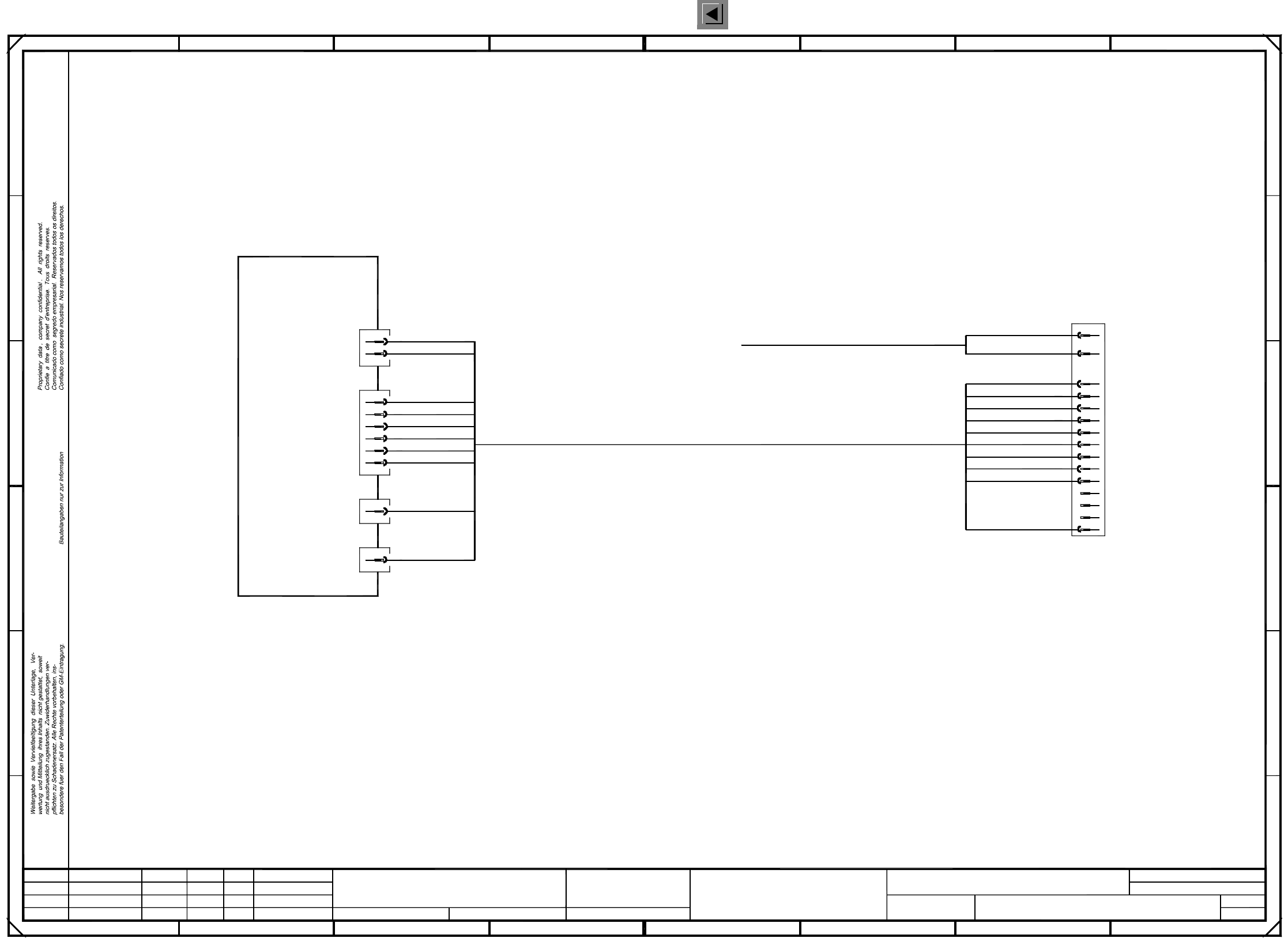
The cable harness for the coplanarity module is part of the cable harness for the control unit !
Please note:
Status Modified Date Name Stand.
Check.
Author
Date
Orig. Creat. f. Creat. by
Supplied with F4B control unit
Power supply
Backplane
bn
rd
pk
wh
wh
wh
wh
wh
wh
pk
wh
bn
wh
wh
bn
wh
rd
wh
wh
pk
pk
wh
(lefthand side)
Fit both wires
to pin 21 of X211
Terminal panel
To
Cable : coplanarity module - terminal panel
Coplanarity module cable harness
=
SIEMENS AG
+
2 Circuit Diagrams 69
I
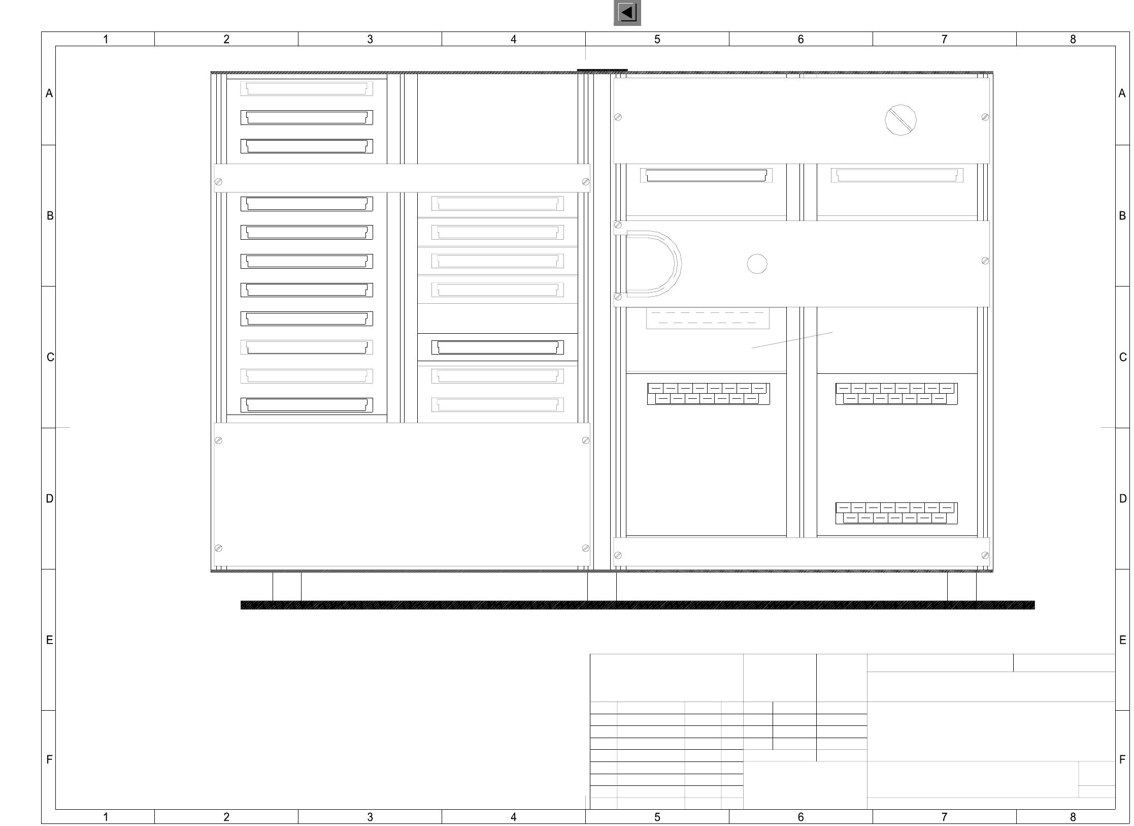
00324341-070101TD3 Supplied with F4B control unit (viewed from the front)
Battery
3.8V
SMD Placement System SIPLACE 80 F4
Sheet
Sh.
(Drawing number)
Main no.
( viewed from the front )
Supplied with F4B control unit
Format
Dimensional variations:
Degree of accuracy
medium
acc. to ISO 2768 mH
Date
Name
Author
Check.
Stand.
Scale
(Material, semifinished products)
(Unmachined part no.)
(Model or swage no.)
NameDateChange noticeStatus
with H15 section
Part of front plate
Copying of this document, and giving it to others and the use
or communication of the contents thereof, are forbidden with-
out express authority. Offenders are liable to the payment of
damages. All rights are reserved in the event of the grant of
a patent or the registration of a utility model or design.
Weitergabe sowie Vervielfaeltigung dieser Unterlage, Verwer-
tung und Mitteilung ihres Inhalts nicht gestattet, soweit nicht
ausdruecklich zugestanden. Zuwiderhandlungen verpflichten zu
Schadenersatz. Alle Rechte fuer den Fall der Patenterteilung
oder GM-Eintragung vorbehalten.
PL EA
SIEMENS
FS ES US UA S F
1
A3
X9sv
X3ts
X2ts
X98
X92
X12su
X11su
X25
X24
X23
X22
X10su
X9su
X8su
X7su
X6su
X5su
X3su
X2su
X1su
1 : 2
00324341-070101TD3
09.12.99
11.11.1999 Tekin
Tek09.12.999182FS07
1
X8sv
X2rz
X1rz
018
X1ts
2 Circuit Diagrams 70
I
00347286-010101FD4 S20/F4B control unit, basic module, wrap connections (Sh. 1 of 3)
00347286-010101FD4 S20/F4B control unit, basic module, wrap connections (Sh. 2 of 3)
Siemens AG
Cable harness
Document number: 00347286-010101FD4
Designation: S20 / F4B control unit, base
PL EA 1 E2
Author : PL EA 1 E6 Ref
Wollgarten
Signature Testing Development Page 1 of 3
Date 29.03.01
S20B / F4B Control unit, Wrap connections incl. M44
SMP16-A12
Coding, axis board 1 (SP5):
Axis no. 0 (module 1)
Axis no. 1 (module 2)
Axis no. 2 (module 3)
B7
⇔
B16
C31
⇔
B19
Coding, axis board 2 (SP6):
Axis no. 3 (module 1)
Axis no. 4 (module 2)
Axis no. 5 (module 3)
C2
⇔
B3
⇔
B4
B16
⇔
B9
C31
⇔
B18
⇔
B20
Coding, axis board 3 (SP7):
Axis no. 6 (module 1)
Axis no. 7 (module 2)
Axis no. 8 (module 3)
C2
⇔
B4
⇔
B5
B16
⇔
B7
⇔
B8
⇔
B9
C31
⇔
B21
Coding, axis board 4 (SP8):
Axis no. 9 (module 1)
Axis no. 10 (module 2)
Axis no. 11 (module 3)
C2
⇔
B3
⇔
B6
B16
⇔
B8
⇔
B10
C31
⇔
B18
⇔
B19
⇔
B21
Interrupt axis boards
SP11/C15
⇔
SP8/C15
⇔
SP8/C17
⇔
SP8/C19 Int. axis 4 on SMP_IREQ3
SP8/C19
⇔
SP7/C19
⇔
SP7/C17
⇔
SP7/C15 Int. axis 3 on SMP_IREQ3
SP7/C15
⇔
SP6/C15
⇔
SP6/C17
⇔
SP6/C19 Int. axis 2 on SMP_IREQ3
SP6/C19
⇔
SP5/C19
⇔
SP5/C17
⇔
SP5/C15 Int. axis 1 on SMP_IREQ3
Siemens AG
Cable harness
Document number: 00347286-010101FD4
Designation: S20 / F4B control unit, base
PL EA 1 E2
Author : PL EA 1 E6 Ref
Wollgarten
Signature Testing Development Page 2 of 3
Date 29.03.01
Coding for I/O-boards 1 - 3 (SMP16-A12):
I/O board 1 SP1/C31
⇔
SP1/C23
⇔
SP1/C25
⇔
SP1/C27
(IREQ9=0 / IREQ10=0 / IREQ11=0)
I/O board 2 SP2 / C31
⇔
SP2 / C23
⇔
SP2 / C25
(IREQ9=0 / IREQ10=0 / IREQ11=1)
I/O board 3 SP3 / C31
⇔
SP3 / C23
⇔
SP3 / C27
(IREQ9=0 / IREQ10=1 / IREQ11=0)
Interrupt I/O boards 1 - 3 (SMP16-A12):
I/O board 1 SP11/C19
⇔
SP1/C15 Int. I/O board 1 SMP-IREQ5
I/O board 2 SP1 / C15
⇔
SP2 / C15 Int. I/O board 2 SMP-IREQ5
I/O board 3 SP2 / C15
⇔
SP3 / C15 Int. I/O board 3 SMP-IREQ5
Communications assembly interrupts:
a. on SMP16-A12 bus
SP11/C21
⇔
SP10/C23 Int CAN bus
SP11/C23
⇔
SP10/C25 Int HS3L
b. between AMS bus and SMP16-A12:
AMS-SP1/C8
⇔
SMP-SP10/C21 Int COM6
AMS-SP1/B8
⇔
SMP-SP10/C19 Int COM5
AMS-SP1/A8
⇔
SMP-SP10/C17 Int COM4
AMS-SP1/C7
⇔
SMP-SP10/C15 Int COM3
AMS bus:
AMS-SP1 / A4
⇔
AMS-SP4 / A3
AMS-SP1 / A3
⇔
AMS-SP1 / B13 (Bus priority)