Detailed Circuit Diagram Folder SIPLACE F5.pdf - 第71页
2 Circuit Diagr ams 71 I 0034728 6-010 101FD4 S 20/F4 B contro l unit , basic m odule, wr ap con nections (Sh. 3 of 3) S i e m e n s A G Cable harness Document number: 0 0 3 4 7 2 8 6 -01 0 1 0 1 F D 4 Designation: S20 /…
2 Circuit Diagrams 70
I
00347286-010101FD4 S20/F4B control unit, basic module, wrap connections (Sh. 1 of 3)
00347286-010101FD4 S20/F4B control unit, basic module, wrap connections (Sh. 2 of 3)
Siemens AG
Cable harness
Document number: 00347286-010101FD4
Designation: S20 / F4B control unit, base
PL EA 1 E2
Author : PL EA 1 E6 Ref
Wollgarten
Signature Testing Development Page 1 of 3
Date 29.03.01
S20B / F4B Control unit, Wrap connections incl. M44
SMP16-A12
Coding, axis board 1 (SP5):
Axis no. 0 (module 1)
Axis no. 1 (module 2)
Axis no. 2 (module 3)
B7
⇔
B16
C31
⇔
B19
Coding, axis board 2 (SP6):
Axis no. 3 (module 1)
Axis no. 4 (module 2)
Axis no. 5 (module 3)
C2
⇔
B3
⇔
B4
B16
⇔
B9
C31
⇔
B18
⇔
B20
Coding, axis board 3 (SP7):
Axis no. 6 (module 1)
Axis no. 7 (module 2)
Axis no. 8 (module 3)
C2
⇔
B4
⇔
B5
B16
⇔
B7
⇔
B8
⇔
B9
C31
⇔
B21
Coding, axis board 4 (SP8):
Axis no. 9 (module 1)
Axis no. 10 (module 2)
Axis no. 11 (module 3)
C2
⇔
B3
⇔
B6
B16
⇔
B8
⇔
B10
C31
⇔
B18
⇔
B19
⇔
B21
Interrupt axis boards
SP11/C15
⇔
SP8/C15
⇔
SP8/C17
⇔
SP8/C19 Int. axis 4 on SMP_IREQ3
SP8/C19
⇔
SP7/C19
⇔
SP7/C17
⇔
SP7/C15 Int. axis 3 on SMP_IREQ3
SP7/C15
⇔
SP6/C15
⇔
SP6/C17
⇔
SP6/C19 Int. axis 2 on SMP_IREQ3
SP6/C19
⇔
SP5/C19
⇔
SP5/C17
⇔
SP5/C15 Int. axis 1 on SMP_IREQ3
Siemens AG
Cable harness
Document number: 00347286-010101FD4
Designation: S20 / F4B control unit, base
PL EA 1 E2
Author : PL EA 1 E6 Ref
Wollgarten
Signature Testing Development Page 2 of 3
Date 29.03.01
Coding for I/O-boards 1 - 3 (SMP16-A12):
I/O board 1 SP1/C31
⇔
SP1/C23
⇔
SP1/C25
⇔
SP1/C27
(IREQ9=0 / IREQ10=0 / IREQ11=0)
I/O board 2 SP2 / C31
⇔
SP2 / C23
⇔
SP2 / C25
(IREQ9=0 / IREQ10=0 / IREQ11=1)
I/O board 3 SP3 / C31
⇔
SP3 / C23
⇔
SP3 / C27
(IREQ9=0 / IREQ10=1 / IREQ11=0)
Interrupt I/O boards 1 - 3 (SMP16-A12):
I/O board 1 SP11/C19
⇔
SP1/C15 Int. I/O board 1 SMP-IREQ5
I/O board 2 SP1 / C15
⇔
SP2 / C15 Int. I/O board 2 SMP-IREQ5
I/O board 3 SP2 / C15
⇔
SP3 / C15 Int. I/O board 3 SMP-IREQ5
Communications assembly interrupts:
a. on SMP16-A12 bus
SP11/C21
⇔
SP10/C23 Int CAN bus
SP11/C23
⇔
SP10/C25 Int HS3L
b. between AMS bus and SMP16-A12:
AMS-SP1/C8
⇔
SMP-SP10/C21 Int COM6
AMS-SP1/B8
⇔
SMP-SP10/C19 Int COM5
AMS-SP1/A8
⇔
SMP-SP10/C17 Int COM4
AMS-SP1/C7
⇔
SMP-SP10/C15 Int COM3
AMS bus:
AMS-SP1 / A4
⇔
AMS-SP4 / A3
AMS-SP1 / A3
⇔
AMS-SP1 / B13 (Bus priority)
2 Circuit Diagrams 71
I
00347286-010101FD4 S20/F4B control unit, basic module, wrap connections (Sh. 3 of 3)
Siemens AG
Cable harness
Document number: 00347286-010101FD4
Designation: S20 / F4B control unit, base
PL EA 1 E2
Author : PL EA 1 E6 Ref
Wollgarten
Signature Testing Development Page 3 of 3
Date 29.03.01
DMA TCP/IP (SMP16-A12)
SP9/B5
⇔
SP11/B19 DMA Request
SP9/B7
⇔
SP11/B18 DMA Acknowledge
SP9/C15
⇔
SP11/A19 Interrupt-LAN
Interrupt GEM computer (SMP16-A5)
SP1/C15
⇔
SP4/C15 IRQ3
SP1/C19
⇔
SP5/C19 IRQ5
SP1/B3
⇔
SP4/B3
⇔
SP5/B3 AEN
Connection between communications assembly and ICOS:
Flat ribbon cable, 20-pin
EMC backplane COM – ICOS backplane
Plug on EMC backplane COM:
b a
1
Pin 1 on b1
2
3
4
5
6
7
8
9
10
✕
Key
11
✕
✕
Pins pinched off
M M
ICOS1 rear panel
X10
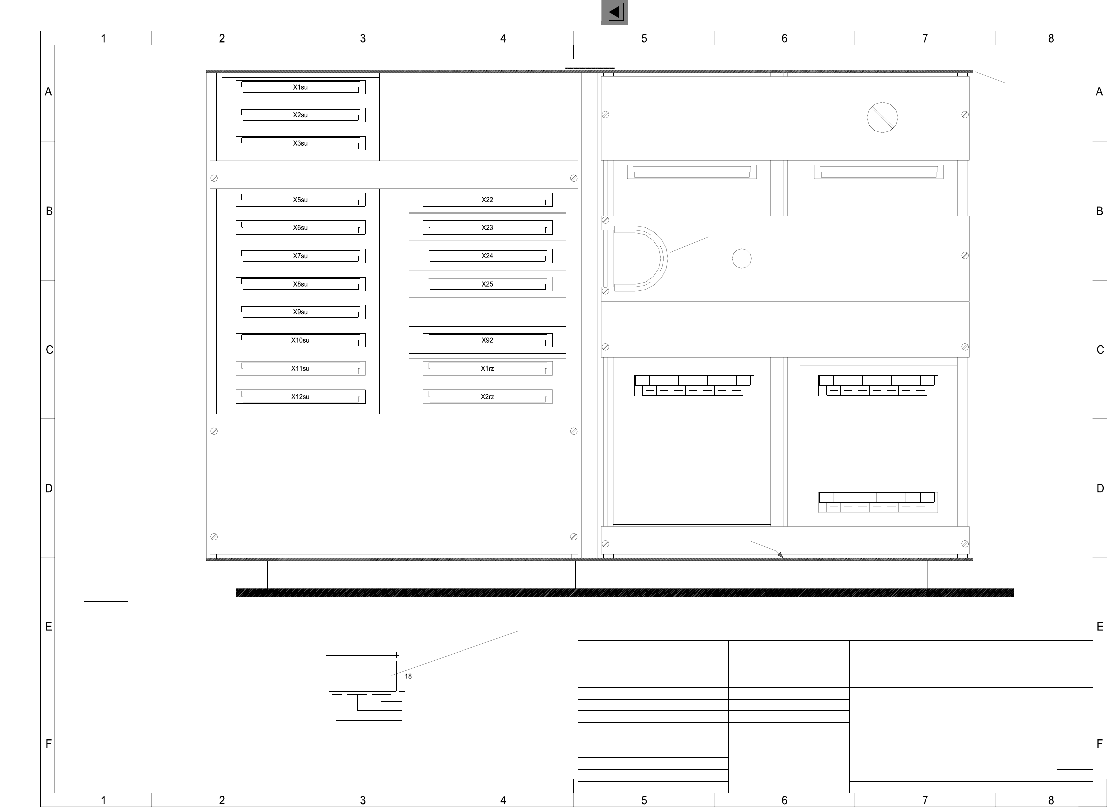
2 Circuit Diagrams 72
I
00347286-010101TD3 S20/F4B control unit, basic module (viewed from the front) (Sh. 1 of 2)
FSUAUSESFS
SIEMENS
PL EA
Weitergabe sowie Vervielfaeltigung dieser Unterlage, Verwer-
tung und Mitteilung ihres Inhalts nicht gestattet, soweit nicht
ausdruecklich zugestanden. Zuwiderhandlungen verpflichten zu
Schadenersatz. Alle Rechte fuer den Fall der Patenterteilung
oder GM-Eintragung vorbehalten.
Copying of this document, and giving it to others and the use
or communication of the contents thereof, are forbidden with-
out express authority. Offenders are liable to the payment of
damages. All rights are reserved in the event of the grant of
a patent or the registration of a utility model or design.
SMD Placement System SIPLACE 80 S20/F4
Sheet
Sh.
Identification: testing engineer, month, yearB: inspection label
Fit labels (flush with front panel)
Assembly inscription acc. to VA-F-510-001
Font size 2.5mm, material Scotchal 3698-E (color Al RAL 9006)
A: identification label
* Please note
Function status (FS) in compliance with the current parts list
Date (year/month/day) acc. to SN 01007
Manufacturer/location acc. to SN 37040
Series number
Status Change notice
neu
Date Name
Dimensional variations:
Degree of accuracy
medium
acc. to ISO 2768 mH
Date
Name
Author
Check.
Stand.
Control unit S20B/F4B, basic module
( viewed from the front )
(Model or swage no.)
(Unmachined part no.)
(Material, semifinished products)
Scale
(Drawing number)
Main no.
Format
SMP bus board
AMS bus board
A35 fan unit (ue)
Edge protection
MVS backplane
Battery
3.8V
* Please note
Power supply backplane
A36
X8sv
1
40
AA-BBBB-CCCC
00347286 / FS
SIEMENS PL EA
S20B / F4B 11.11.99 Tek
Tekin11.11.1999
11.11.99
00347286-010101TD3
1 : 2
A32
X1ts
A27
X2ts
X3ts
X9sv
A33
A3
2
006
005
002
003
004
005
001