80S20 circuit.pdf - 第107页
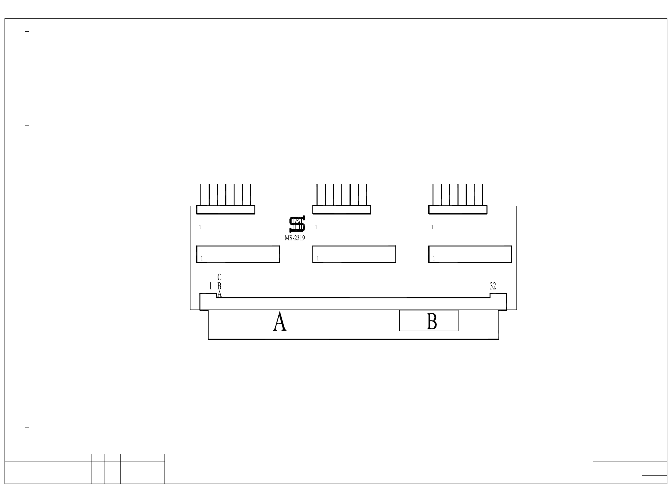
5 SIPLACE 80S-20 Printed Circuit Boards 107 00319076-020102ND3 Axis rear panel (axis 166) The following labels have to be stuck on ! A: Identification label X6 X5 00319076-020102ND3 2. 2. 27.09. 95 27.09. 95 Sz Sz 319078…
5 SIPLACE 80S-20 Printed Circuit Boards 106
00300398-030105ND4 Gantry distributor board
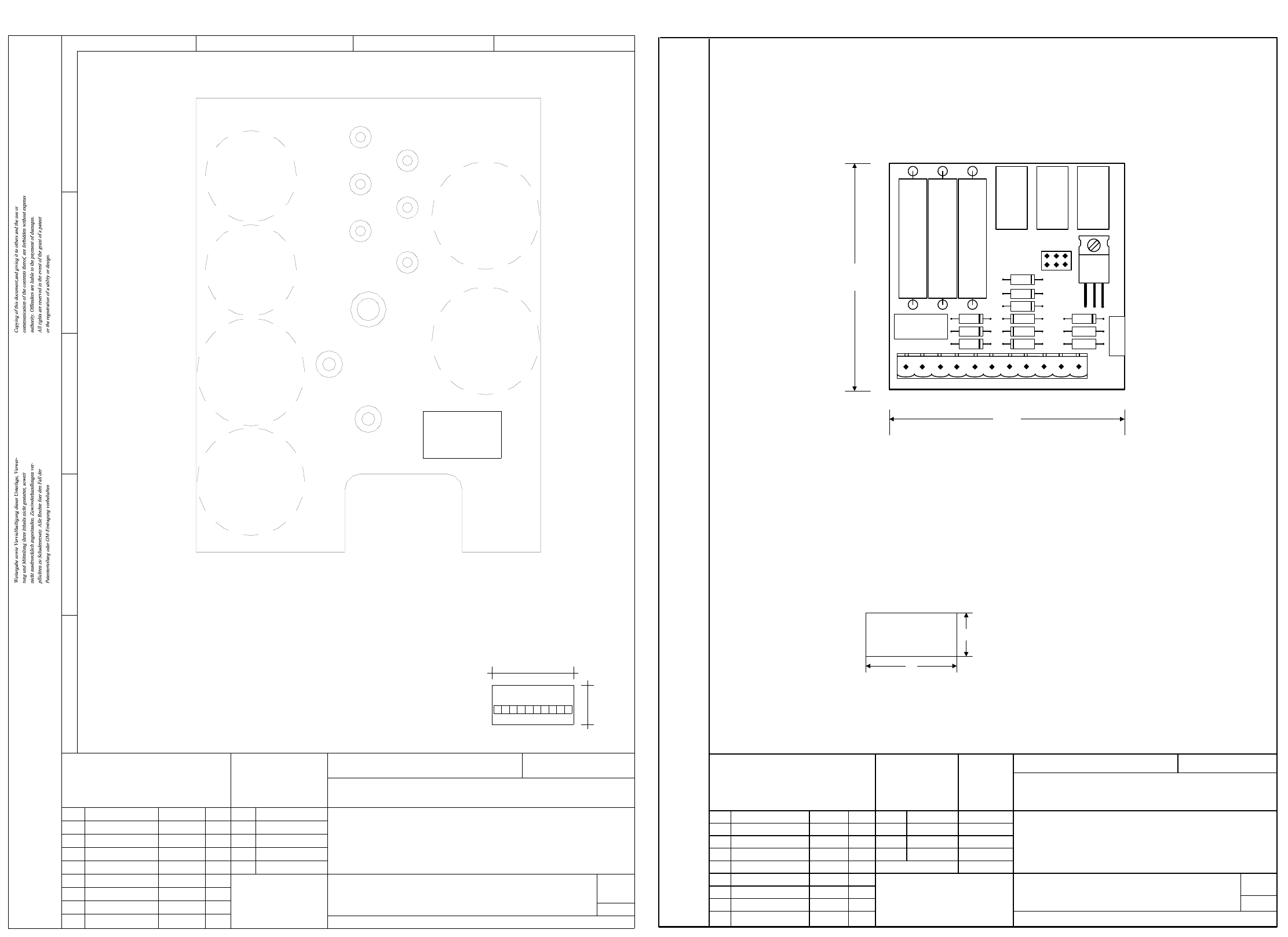
00308443-050101ND4 Discharge board
C2
C3
C4
C5
C6
Ident.
AA-BBBB-CCCC
SIEMENS AUT 5
123456789
15
30
00300398
BBBB Date (year/month/day) according to SN 01007
Max. component height 50 mm
Max. clamping height 52 mm
PCB size 145*109*3 mm
1710460-Y0026-000-03-N
CCCC Numerals
AA Manufacturer/location according to SN 37040
00300398
Y0026N04
4321
E
D
C
B
A
AUT 5
SIEMENS
Product status
Doc. status
1
1
SMD Placement System Siplace
Stat. Modified Date Name
Date
Author
Check.
Stand.
Mat.-Nr. :
Scale
Sheet
Sh.
CAD file:
Sz
00300398-030105ND4
Potential distribution board
4. 9.10.95 Tu.
3. 22.6.93 Sz.
28.01.1992
The following identification label has to be stuck on:
Font size 2.5 mm, material Scotchcal 3698-E (color Al RAL 9006)
Assembly inscription according to recommendation VA-F-510-001AUT5
1
2
3
5
7
8
9
4
6
+8/55V
+30V switch.
+24V
+30V
+12V
+5V
GND
8/55V
8/85V
C1
1.
5.
1.
28.05.96
28.05.96
28.05.96 Tu.
Tu.
Tu.
28.05.1996
28.05.1996
00308443-050101ND4
SIEMENS
Aktiengesellschaft
AUT 5 BPB BS1
Date
Author
Check.
Stand.
Name
File name:
Stat.
Modified
Date
Name
(Drawing number)
Format A4
Drw. no.: FS PS DS S/F
Sheet
Scale
Weitergabe sowie Vervielfältigung dieser Unterlage, Verwertung und Mitteilung ihres
Inhaltes nicht gestattet, soweit nicht ausdrücklich zugestanden. Zuwiderhandlungen
verpflichten zu Schadenersatz. Alle Rechte für den Fall der Patenterteilung oder GM-
Eintragung vorbehalten.
Copying of this document, and giving it to others and the use or communication of the
contents thereof, are forbidden without express authority. Offenders are liable to the
payment of damages. All rights are reserved in the event of the grant of a patent or the
registration of the utility model or design.
(a1_1zu1.vsd)
00308443-050101ND4.vsd
75 mm
72 mm
1/1
R1
K1
R2 R3
K2 K3
V3 V8
V4
V5
V7
V6
V11
V10
V9
V2
R4
R5
A
B
X1
X2
V1
1
Old drawing no.: 1710470-Y0034-000-04
Siemens AUT5
00308443-05
AA-BBBB-CCCC
15
10
Function status
Document status
Product status
SMD Placement System Siplace
Discharge board
The following labels have to be stuck on:
A: Identification label
B: Inspection label
Assembly inscription acc. to recommendation VA-F-510-001
font size 1.5 mm, mat. Scotchcal 3698-E ( color A1 Ral 9006 )
AA = manufacturer/location acc. to SN 37040
BBBB = date (year/month/day) acc. to SN 01007
CCCC = numeral
Product inspection certification acc. to recommendation VA Q 509-001
5 SIPLACE 80S-20 Printed Circuit Boards 107
00319076-020102ND3 Axis rear panel (axis 166)
The following labels have to be stuck on !
A: Identification label
X6
X5
00319076-020102ND3
2.
2.
27.09.95
27.09.95
Sz
Sz
319078-02
12.01.1995
Dax
Axis rear panel
(axis 166)
AUT5-BSM
Siemens AG
Stromlaufplan/Circuit diagram
19181716151413121110987654321
Product status
Doc. status
SMD Placement System Siplace 80S20
1
1
Status DateModified Name Stand. Orig./Repl.f/Replaced by
Check.
Date
Author
Mat. no.:
Sh.
Sh.
Maximum component height: top = 9.0 mm; bottom = 2.0 mm
B: Inspection label
X2
X1
X4
X3
X7
5 SIPLACE 80S-20 Printed Circuit Boards 108
00320854-020202MD4 745 PCB, backplane-servo unit Y1002
00320855-010202MD4 Backplane-servo unit Y1003
Function status
Product status
Doc. status
02
02
02 15.04.96
15.04.96 DO
DO
SIEMENS AG
FSZ MUENCHEN
MS-Dorn
03.07.95
00320854-020202MD4
backplane - servo Y1002
745 printed circuit board
SIPLACE
Sheet
1-
Component diagram, bottom
ANL A441 TD FSZ E
DO15.04.96
Component diagram, top
Wire infeed
Apply the following labels:
A: Identification label
Max. component height:
B: Inspection label
Top = 19mm
Bottom = 34 mm
Remove pins marked 'x'
Stat. Modified Date Name
Date
Name
Scale 1:1
Product status
Doc. status
02
02 03.06.97
03.06.97 Tek
Tek
SIEMENS AG
AUT5-BSM
Goller
26.09.1995
00320855-010202MD4
backplane - servo Y1003
SIPLACE
Sheet
1-
Component diagram, bottom
Component diagram, top
Apply the following labels:
A: Identification label
Max. component height:
B: Inspection label
Top = 51 mm
Bottom = 20 mm
Remove pins marked 'x'
Stat. Modified Date Name
Date
Name
X3
1
X8
X2
X7
X6
X5
1
X4
1
1
1
X7
*)
+
Wire infeed
X1
*) C1 option only
not inserted!
Scale 1:1