00193161-01.pdf - 第72页
Placement of 0 402 components Manual S-20/S-23 HM/S-25 HM/F4/F5 HM/HS-50 03/2001 edition 72 10 Solderin g When sma ll compo nents are s oldered, there is a r isk of the tombst oning effect, i. e. the compo nents are pull…

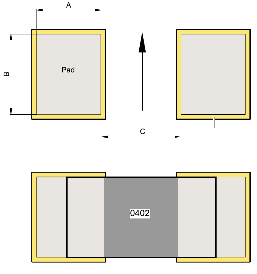
Manual S-20/S-23 HM/S-25 HM/F4/F5 HM/HS-50 Placement of 0402 components
03/2001 edition
71
PLEASE NOTE:
If you are not using laser-cut metal stencils and do not follow the rule of thumb for the shape of
the apertures, peaks of solder paste can form when you remove the stencil. 9
The solder paste is generally approximately 125 µm (5 mil) thick. If the apertures are of the wrong
shape or have rough surfaces, the adhesive strength of the solder paste increases, which means
that it does not easily come away from the walls of the aperture when the stencil is lifted. The
solder paste is then pulled up with the stencil. This can create peaks up to 300 µm high before the
solder paste finally tears away from the stencil.
If the stencils are too thick, the solder paste can ball together, thus causing short-circuits.
Recommendations for:
Stencil thickness / solder paste thickness150 µm (= 6 mil)
Stencil thickness / solder paste thickness125 µm (= 5 mil) 9
9.3 Solder paste
Standard solder paste generally has a grain size of 45 – 75 µm (type 3). To guarantee a smooth
and efficient placement process, we recommend the use of a fine pitch paste with a grain size of
20 - 45 µm (type 4).
Placement of 0402 components Manual S-20/S-23 HM/S-25 HM/F4/F5 HM/HS-50
03/2001 edition
72
10 Soldering
When small components are soldered, there is a risk of the tombstoning effect, i.e. the
components are pulled up vertically on one side, giving them the appearance tombstones.
Tombstoning can be caused by placement offset in the longitudinal direction, uneven heating of
the soldered connection or an unsuitable pad layout.
10.1 Basic principles of the soldering process
Both component connections and the solder paste deposit should be evenly heated, and reach
melting point at the same time. Commercially available solder (Sn63Pb37) melts at a fixed melting
point of 183 °C, and not within a melting range of 183 °C – 190 °C, for example, as is the case
with Sn60Pb40. If the two soldered connections do not reach melting temperature at the same
time, then the solder liquefies first on the hotter side. The resulting surface tension of the molten
solder then pulls the component up vertically like a tombstone.
This effect is more noticeable with capacitors than with resistors, since capacitors are easier to
pull vertically since they have a larger end surface.
10.2 Points to note during soldering
During soldering, be careful to distribute the air flow of a forced convection oven evenly over the
PCB - on both the underside and the topside - in order to minimize differences in temperature.
Manual S-20/S-23 HM/S-25 HM/F4/F5 HM/HS-50 Placement of 0402 components
03/2001 edition
73
10.3 Pad layout
A good pad layout greatly reduces the risk of tombstoning. Use pads as shown in the drawing
below, rather than square pads.
Fig. 10 - 1 Pad layout for 0402 components
Recommended transport direction
during wave soldering
Solder resist