00193161-01.pdf - 第74页
Placement of 0 402 components Manual S-20/S-23 HM/S-25 HM/F4/F5 HM/HS-50 03/2001 edition 74 10.4 Recommended p ad layout Å Reduce the siz e of the ste ncil ape rture by 0 .03 mm. Å Increas e the size o f the sold er resi…
Manual S-20/S-23 HM/S-25 HM/F4/F5 HM/HS-50 Placement of 0402 components
03/2001 edition
73
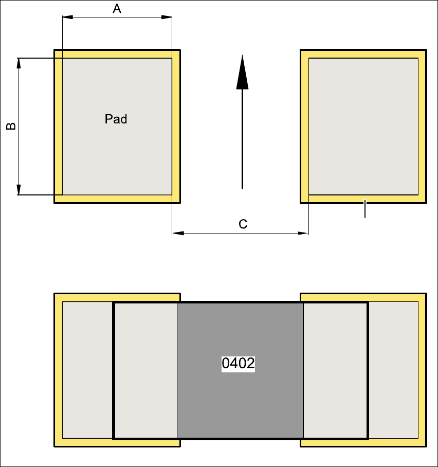
10.3 Pad layout
A good pad layout greatly reduces the risk of tombstoning. Use pads as shown in the drawing
below, rather than square pads.
Fig. 10 - 1 Pad layout for 0402 components
Recommended transport direction
during wave soldering
Solder resist
Placement of 0402 components Manual S-20/S-23 HM/S-25 HM/F4/F5 HM/HS-50
03/2001 edition
74
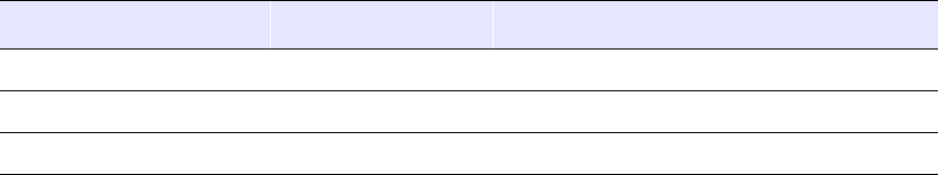
10.4 Recommended pad layout
Å Reduce the size of the stencil aperture by 0.03 mm.
Å Increase the size of the solder resist by 0.05 mm.
Component A B C
0402 0.40 0.61 0.59
Standard 0402 0.43 0.45 0.51
Mini 0402 0.43 0.44 0.51