YesAX V3.1.2 - Software User Manual - 第115页
General Inspecti on Methodolo gy 10 - 21 the Show Edge Map box can be checked so that each time P1 or P2 has been changed; the updated edge map will show on screen. This way the user will have a better idea a bout how P1…
10-20 General Inspection Methodology
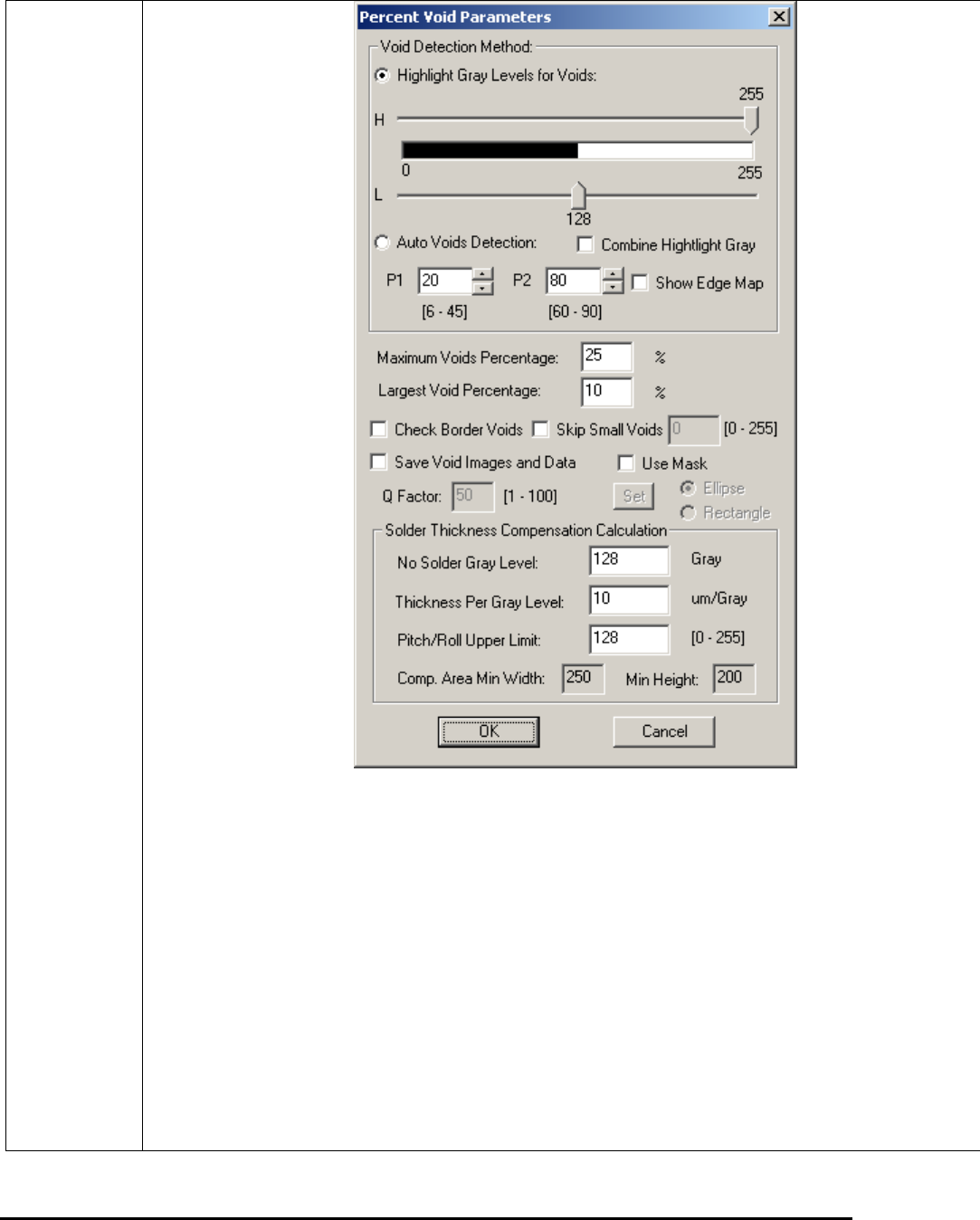
The Highlight Gray Levels for Voids enables the user to highlight a range of gray scale values
that include the feature of interest. These highlighted pixels will be considered “lit” during the
Percent Void computation.
The Auto Voids Detection applies edge detection techniques to find voids. There are two
parameters for this function: P1 and P2. P1 is the indicator for a Gaussian Median filter and P2
represents one high threshold value. The normal range for P1 is from 6 to 45 and the range for
P2 is from 60 to 90, as shown under each box. For most applications you may set P1 somewhere
between 12 and 24 and set P2 between 70 and 80. The default values for P1 and P2 are 20 and
75, correspondingly.
To adjust these two parameters, you should always start with P1 and pay more attention on this
one since this is the one that affects final result more. Increasing the value of either P1 or P2, you
tend to lose small voids and in the mean time, get rid of un-wanted noise. Try not use very low
value for P1 when image noise level is high. Also be noticed that increasing P2 too much may
break the contour line of some voids and create some irregular shapes. To help tuning P1 and P2,
General Inspection Methodology 10-21
the Show Edge Map box can be checked so that each time P1 or P2 has been changed; the
updated edge map will show on screen. This way the user will have a better idea about how P1
and P2 work. Uncheck the Show Edge Map box, the void result will show on screen again. If
the image noise level is high, to make auto void detection works better, it is preferable for user to
apply Median Filter as pre-processing for solder inspection.
Sometimes it is useful to combine the results of highlight gray and auto voids detection together.
To make it happen the user needs to adjust parameters for both highlight gray and auto voids
detection first. Then check the Combine Highlight Gray box.
The Maximum Voids Percentage sets a pass/fail percentage for the Percent Void inspection.
This threshold will represent the passing ratio of the number of the lit pixels over the total
number of the pixels in the window of interest. If the actual ratio is high, the test result will fail.
The Largest Void Percentage sets another pass/fail percentage for the Percent Void inspection.
The value of Largest Void represents the acceptable ratio of the number of pixels in the largest lit
blob over the total number of pixels in the window of interest. If the ratio is high, the test result
will fail.
The Check Border Voids option, if enabled, will look for all voids connected to border of solder
inspection box and include them in the percent void calculation. If this item’s been disabled, any
voids connected to border will be ignored.
The Skip Small Voids option, if enabled, will ignore any void size smaller than the preset value.
If the image is noisy, sometimes those small voids been found are noise of the image rather than
the true voids. This is to diminish the impact of image noise to percent void calculation. The void
size is counted in pixels and the range of threshold is between 0 and 255.
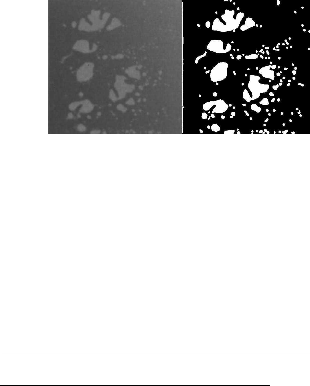
The Save Void Images and Data option, if enabled, will save the original solder image together
with the detected void image in one file with the name of that part ref id. All void images saved
during inspection will be put to the same folder with the name of current board serial number.
This folder is saved under VoidImage folder inside the current recipe folder. Below is one
example of the void image. The original image is at left and the void result is at right. This is a
good tool for customers who want to store the void detection results. The Q Factor field is used
to control the image quality of the saved void image. When it is set to 100, the void image will
be saved as the highest (uncompressed) quality. When set to 1, the void image will have the
lowest quality.
10-22 General Inspection Methodology
The Solder Thickness Compensation Calculation is for solder thickness compensation
purpose. It won’t be enabled if the following two fields: No Solder Gray Level and High
Pitch/Roll Threshold are filled with 0 or the solder inspection box has a width less than Comp.
Area Min Width (250 in pixels) or a height less than Min Height (200 in pixels). In reality the
solder thickness of a solder joint is not even. For example, if the component is tilted in one way,
then along that direction the thickness of the solder area will gradually increase or decrease,
which causes the unevenness of the image. If a void is located at relatively thick solder area, it
may even appears darker than some thin solder areas without any void at all. This will make void
detection more difficult. The solder thickness calculation is designed to compensate for the
unevenness of the solder layer.
To make it work, first the user needs to set up the No Solder Gray Level, which represents the
average gray levels for areas without any solder. To set up Thickness Per Gray Level, some
calculation needs to be done first. If the thickness of solder is 500µm (this number can be
acquired by doing laser height measurement on solder area), and the gray levels for such amount
of solder is 50, then the Thickness Per Gray Level will be 10µm/Gray (500/50). Once the pitch
and roll have been calculated, the results will be compared with High Pitch/Roll Threshold
first. Only numbers bigger than the preset threshold value will be used for thickness
compensation. If the numbers are smaller, it is reasonable to assume that the numbers are not
reliable thus the user will choose rather not doing the compensation at all. The results of Pitch
and Roll can be seen on the percent void result dialog, together with the inspection results.
Sometime there is certain area inside the ROI that the user does not want to inspect. To mask out
the area the user can enable the Use Mask option, select either Ellipse or Rectangle as shape
indicator and then click Set button to define the mask area. The mask area does not need to be
totally reside inside the ROI and the mask out area will be subtracted from the total area
calculate.
Solder Alignment.
Move/Resize
Moves and/or Resizes the solder inspection box.
Delete
Deletes the current solder.