YesAX V3.1.2 - Software User Manual - 第120页
10 - 26 General Inspecti on Methodolo gy X-ray Solder inspection uses a threshold value to binarize the image into black or w hite pixels. The user can select to use either a fixed Threshold value (by moving the slider b…
General Inspection Methodology 10-25
The Check Center Spot is for AOI inspection and should not be enabled for X-Ray inspection.
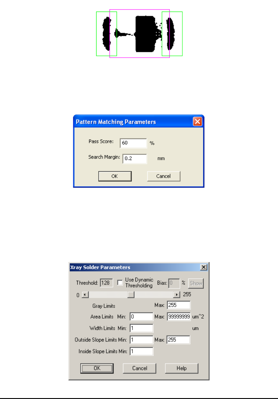
10.4.3 Pattern Matching Parameters
Select Pat Match Param.. from the Solder pop-up menu to open the Pattern Matching
Parameters dialog.
Pattern matching is more commonly used in Mark inspection, but can also be used in solder
inspection. The idea is to use a known “good” solder joint as a template to check the others
against. During inspection the image of every joint is compared to the template and joint images
(defined by the pass score) are rejected.
10.4.4 X-Ray Solder Parameters
Select X-ray Solder Setup from the Solder pop-up menu to open the Xray Solder Parameters
dialog.
10-26 General Inspection Methodology
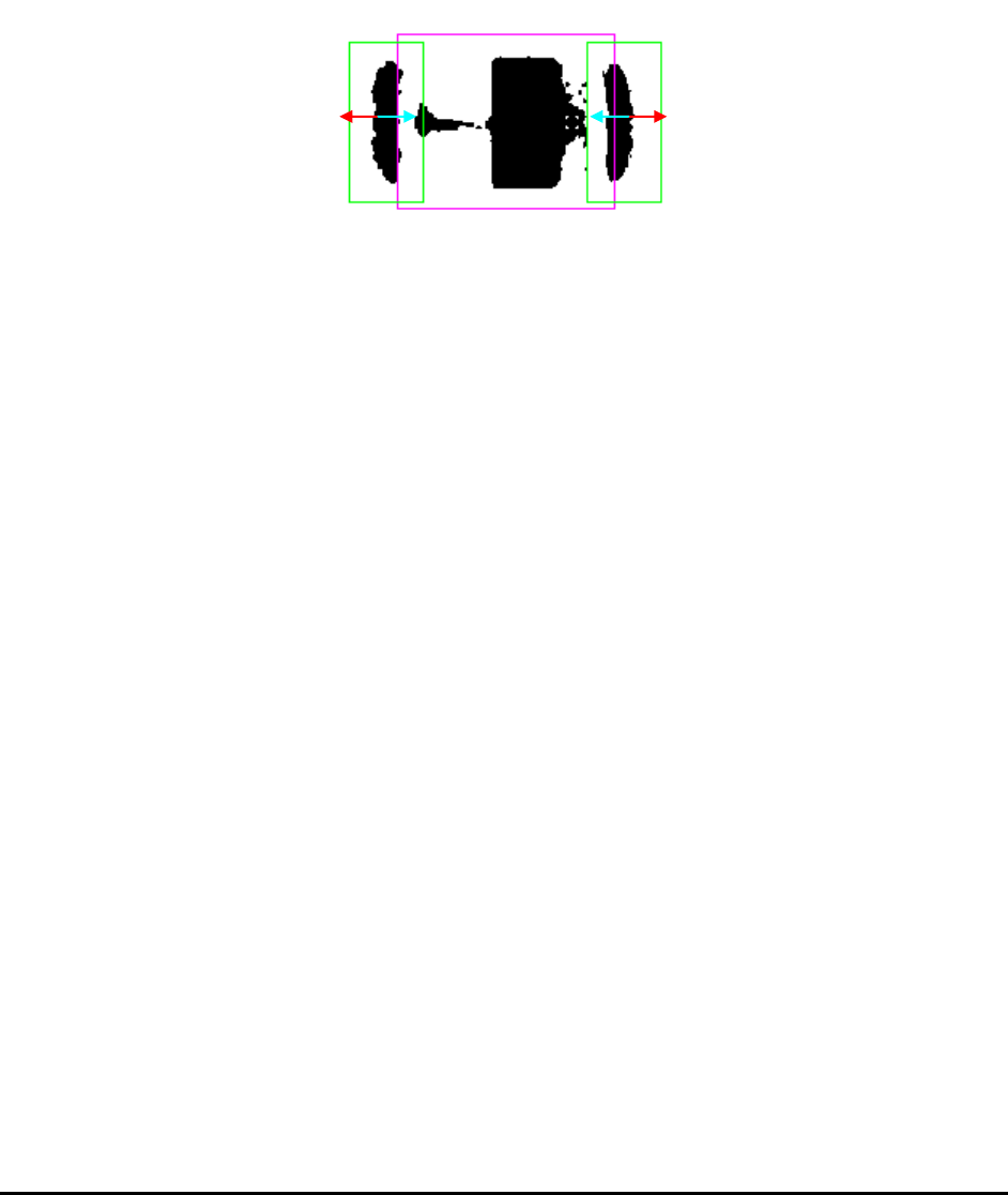
X-ray Solder inspection uses a threshold value to binarize the image into black or white pixels.
The user can select to use either a fixed Threshold value (by moving the slider bar left and right)
or use a dynamic threshold (by putting a number in the Bias field). The Bias field and the Show
button will only be enabled if the user checks the Use Dynamic Thresholding field. The black
area in the middle of inspection box will be detected as the main solder area of resistor pins. The
average gray level, the area and the width of this area will be calculated. The numbers will be
compared with the following threshold values: maximum gray level, minimum area, maximum
area and minimum solder width. Any number outside the range indicates a solder defect.
In the meantime the algorithm will scan the middle section of the solder area and calculate the
maximum outside slope and maximum inside slope. Here the slope refers to differences of gray
levels of neighboring pixels along a specific direction. From center of solder area towards
outside of the device a maximum outside slope (the red arrow above) value will be calculated
and towards inside of the device a maximum inside slope (the cyan arrow) value will be
calculated. The solder has missing or insufficient defect will have a relatively small inside and
outside slope value. The minimum outside slope and minimum inside slope are two thresholds
used to separate the bad solder joints from the good ones.
In X-ray view, X-ray solder inspection can effectively detect missing, insufficient or excess
solder for capacitors and other devices having a similar shape in X-ray view.
10.4.5 Solder Blob Analysis Parameters
The solder blob analysis algorithm can be used (amount other applications) to detect solder balls
around the chip components.
Select Solder Blob Params from the Solder pop-up menu to open the Solder Blob Analysis
Parameters dialog.
General Inspection Methodology 10-27
Similar to Xray Solder inspection, the Solder Blob Analysis uses a threshold value to binarize the
image into black or white pixels. The user can select to use either a fixed Threshold value (by
moving the slider bar left and right) or use a dynamic threshold (by putting a number in the Bias
field). The Bias field and the Show button will only be enabled if the user checks the Use Thresh
field.
The Count Limits Min and Max set the acceptable blob count. The Area Limit Min sets the
minimum area of the blob. Blobs smaller than the minimum area will not be counted as a blob.
The Size Limits field sets the acceptable size (width or height) of the blobs.
To detect a solder ball around chip components the Count Limit Min and Max should both be
set to 0s. The Area Limits Min should be set to the minimum area of the solder ball that is
considered a defect. The Invert Image checkbox should be checked to make a black solder ball
appear as a white blob.