FCM_User Reference Manual.pdf.pdf - 第271页
4022 591 960 82 Us er Reference Man ual 02.02 FC M Multif lex 6-79 Pr oduc t Ch ang e Ov er ▼ For w hich components d o you use this algo rithm F or compo n ent s that have a good r eflection image (lea d ends, or body )…
Product Change Over
User Reference Manual 4022 591 96082
6-78 FCM Multiflex 02.02
▼ For which components do you use this algorithm
For components that do not have a good reflection image (lead ends, or body), like:
• Transformer coils, 0402, 0603, etc.;
• Tantals with no good reflection (brown, dark colours);
• MELFs with no good reflection (black colour).
▼
General important information
• This algorithm is not as critical as the CHIP algorithm.
• The ruler offsets are fixed; this means that they are not adjustable in the SMD
info file.
The CHIP algorithm
▼ How does it work
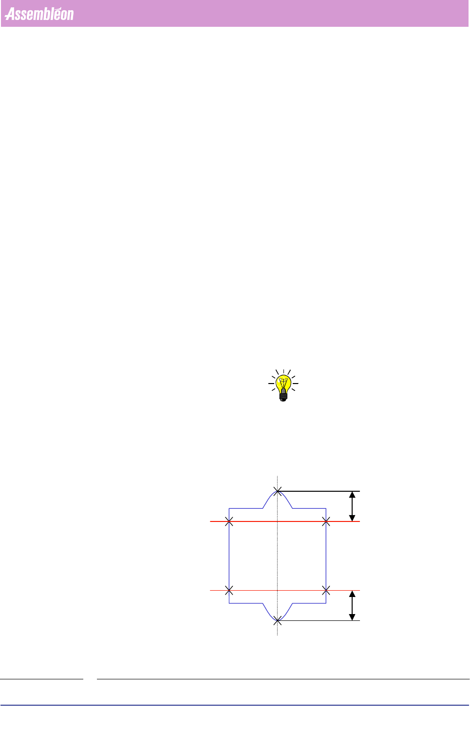
1. Find the rough centre and angle of the reflecting areas.
2. Measure the North-South vertical size, and update the vertical component
centre’s position.
3. Find the edges by the North-South ruler, and place the horizontal rulers with a
ruler offset.
4. Measure the horizontal size of the component’s North side.
5. Measure the horizontal size of the component’s South side.
NOTE: To find a component with the CHIP algorithm, all six crosspoints must be
correct!
FIGURE 6-28 The CHIP algorithm measuring aspects
Ruler
Ruler
Ruler-Offset
Ruler-Offset
NORTH
SOUTH
4022 591 96082 User Reference Manual
02.02 FCM Multiflex 6-79
Product Change Over
▼ For which components do you use this algorithm
For components that have a good reflection image (lead ends, or body), like:
• 0402, 0603, etc.;
• Yellow tantals;
• MELFs with good reflection.
▼
General important information
• This algorithm is more critical than the RECTANGLE algorithm. This means it
needs a better/sharper vision image of the component.
• Ruler offsets are adjustable in the SMD info file; normally the value 3 is used
for most components (5 or 7 is also possible if you have components with a
bigger lead width). Ruler offset is in pixels; one pixel = 75x 75 µm. Always
use odd ruler widths in order to get valid mean calculation results.
The SOT algorithm
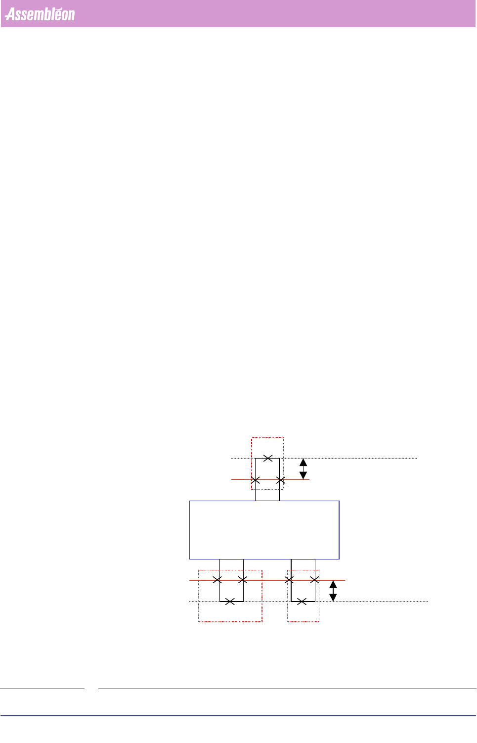
▼ How does it work
1. Find the first and last lead of the South side (for a SOT, normally more than one
lead).
2. Find the first and last lead for the other side.
3. Measure all lead sides (edges) for both component sides (North/South).
4. Measure all lead ends for both component sides (North/South).
5. Chech the pitch between the leads (if there is more then one lead a side).
FIGURE 6-29 The SOT algorithm measuring aspects
Ruler
Ruler
Ruler offset
Ruler offset
Lead edge
Lead end
Search area Fine-search area
Fine-search area
SOUTH
NORTH
Product Change Over
User Reference Manual 4022 591 96082
6-80 FCM Multiflex 02.02
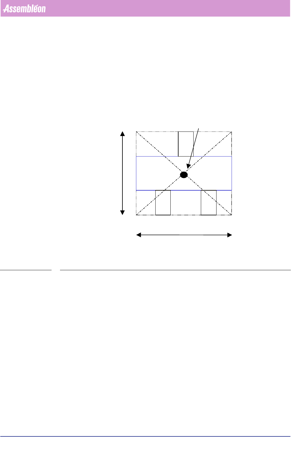
6. Calculate the centre and angle of the component with the information of the
lead sides and lead ends.
7. Check the distance between the middle of the first side (North) to the middle of
the second side (South).
8. Calculate the component origin, based on the found vision origin and gravity
offsets.
FIGURE 6-30 Calculation of the component origin
▼
For which components do you use this algorithm
For components that have leads on two sides (North and South), having only one
lead at one side, like:
• Transistors SOT23, SOT323, etc.;
• DPAKs.
▼
General important information
• Ruler offsets are adjustable in the SMD info file; normally the value 3 is used
for most components (5 or 7 is also possible if you have components with a
bigger lead width). Ruler offset is in pixels; one pixel = 75x 75 µm. Always
use odd ruler widths in order to get valid mean calculation results.
• The body length and width in the SMD info file must be correct, because they
determine the positions of the leads together with the number of leads and
the lead pitch.
• For the ruler threshold, the value is normally between 20 and 30, but it
depends on the specific component type and the amount of light used.
Component origin = vision origin
NORTH
SOUTH
Body length
Body width